Photonic crystal and thin film piezoelectric sonic sensor

A phononic crystal and piezoelectric acoustic wave technology, applied in the field of sensors, can solve the problems of not being able to effectively improve the quality factor of thin-film piezoelectric acoustic wave sensors and energy limitations, and achieve the effects of limiting energy dissipation, high quality factor, and efficient reflection

Active Publication Date: 2019-09-24
SUZHOU INST OF BIOMEDICAL ENG & TECH CHINESE ACADEMY OF SCI
View PDF7 Cites 8 Cited by
  • Summary
  • Abstract
  • Description
  • Claims
  • Application Information

AI Technical Summary

Problems solved by technology

[0004] Therefore, the technical problem to be solved by the present invention is to overcome the limitation of the energy reflected by the thin-film piezoelectric acoustic wave sensor provided with phononic crystals in the prior art, and the defects that the quality factor of the thin-film piezoelectric acoustic wave sensor cannot be effectively improved

Method used


Image

  • Photonic crystal and thin film piezoelectric sonic sensor
  • Photonic crystal and thin film piezoelectric sonic sensor
  • Photonic crystal and thin film piezoelectric sonic sensor

Examples


Embodiment 1

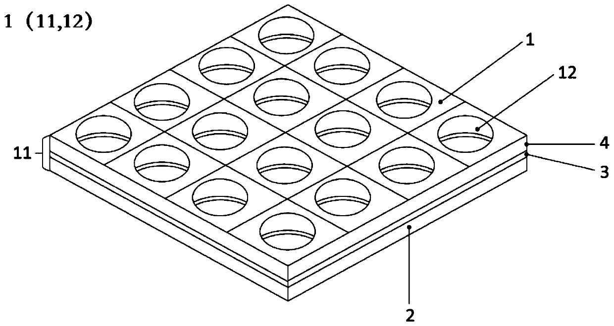
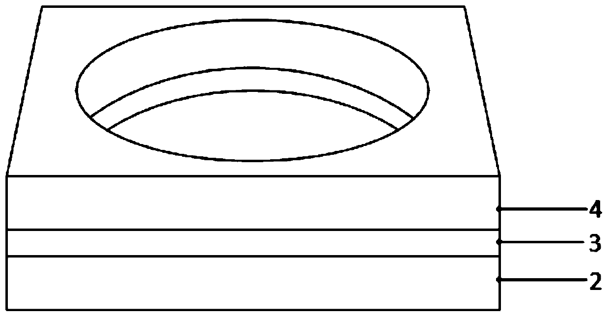
[0053] This embodiment provides a phononic crystal 1 . The phononic crystal 1 is composed of a base 11 and a scatterer 12 formed on the base 11 . Such as figure 1 and figure 2 As shown, the matrix 11 of the phononic crystal 1 is a composite dielectric layer formed by sequentially stacking three dielectric layers of the piezoelectric layer 4, the ground electrode layer 3 and the substrate layer 2; The periodically arranged through holes form the scatterer 12 of the phononic crystal 1 .

[0054] Specifically, such as figure 2 In the shown unit cell phononic crystal 1, the through hole is a cylindrical hole that runs through the composite phononic crystal 1, figure 2 The smallest periodic structural unit of phononic crystal 1 is shown in . The single-cell phononic crystals 1 are arranged in a square lattice, forming as figure 1 The shown phononic crystal 1 has through-holes arranged periodically, wherein the through-holes extend along the length and width directions of th...

Embodiment 2

[0072] This embodiment provides a thin film piezoelectric acoustic wave sensor, such as Figure 11 As shown, it includes a substrate layer 2 , a ground electrode layer 3 and a piezoelectric layer 4 stacked in sequence, and at least one interdigital transducer 5 is provided on the side of the piezoelectric layer 4 away from the ground electrode layer 3 . For example, the thin-film piezoelectric acoustic wave sensor is a two-port type, and the side of the piezoelectric layer 4 away from the ground electrode layer 3 is horizontally oppositely provided with two transducers 5 , namely an input transducer and an output transducer. The transducer 5 is specifically an interdigital transducer 5, and the input transducer and the output transducer correspond to the input interdigital transducer and the output interdigital transducer respectively. The two sides of the transducer 5 are respectively provided with phononic crystals 1, that is, on the side where the input IDT is facing away f...

experiment example 1

[0085] This experimental example tests the phononic crystal 1 formed on the aluminum nitride layer, molybdenum layer and silicon substrate layer in the thin-film piezoelectric acoustic wave sensor of Example 2, and the phononic crystal 1 formed only on the silicon substrate layer in the thin-film piezoelectric acoustic wave sensor of Comparative Example 1 The phononic crystal 1, the improvement effect of the acoustic wave transmission loss in the thin film piezoelectric sensor, is as follows:

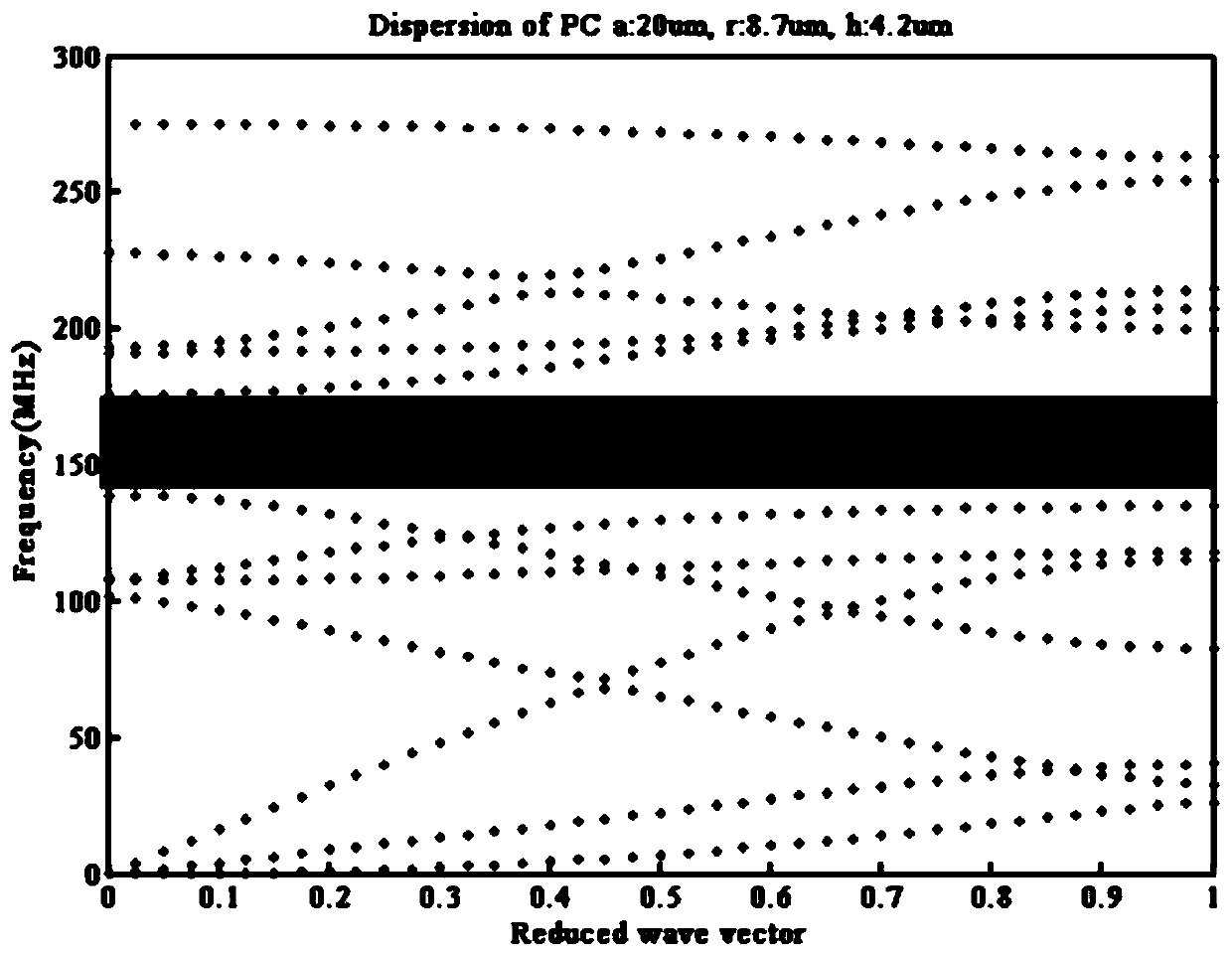
[0086] 1. Adjust the filling rate of the phononic crystal 1 (that is, the area of ​​the cylindrical through hole / the area of ​​the square lattice), and detect the change of the bandgap width of the phononic crystal 1 in the thin-film piezoelectric acoustic wave sensor. The results are as follows Figure 13 as shown, Figure 13 middle f 1 represents the lower edge frequency of the band gap of phononic crystal 1, f 2 Represents the upper edge frequency of the bandgap of phononic crystal...


PUM


Abstract

The invention discloses a thin film piezoelectric sonic sensor. The thin film piezoelectric sonic sensor comprises a substrate layer, a ground electrode layer and a piezoelectric layer which are arranged in a laminated mode, and one or more transducers are arranged on the side, away from the ground electrode layer, of the piezoelectric layer; and photonic crystals at least formed in the piezoelectric layer are correspondingly arranged on the two sides of the transducers, and the resonant frequency of the thin film piezoelectric sonic sensor is located in band gaps of the photonic crystals. According to the thin film piezoelectric sonic sensor, the photonic crystals are at least arranged on the piezoelectric layer, the mechanical vibration stability of the piezoelectric layer is improved, the sonic wave reflectivity is improved, the energy loss of sonic wave transmission is lowered, and the quality factor of the sensor is improved. The invention discloses a photonic crystal. The photonic crystal comprises a matrix and a scatterer formed on the matrix, the matrix is formed by at least two media layers in a laminated mode, and materials of any one of the media layers are different from those of other media layers. According to the photonic crystal, the sonic wave energy loss can be effectively reduced, and the quality factor of the sensor can be effectively improved when the photonic crystal is applied to the thin film piezoelectric sonic sensor.

Description

technical field [0001] The invention relates to the technical field of sensors, in particular to a phononic crystal and a thin-film piezoelectric acoustic wave sensor. Background technique [0002] Piezoelectric film can realize the conversion between electrical energy and mechanical energy by using its piezoelectric effect. Thin-film piezoelectric acoustic wave sensor uses high-performance thin-film piezoelectric materials and rapidly developing micro-nano manufacturing technology to greatly reduce the effective resonance mass of the sensor. , the operating frequency is constantly increasing, and the detection sensitivity is comparable to that of optical sensors. Not only that, because the manufacturing process of the thin-film piezoelectric acoustic wave sensor is compatible with the CMOS process, it is more convenient for integration and mass production, and has broad application prospects in various modern electronics, communication technology, analysis and detection fie...

Claims


Application Information

Patent Timeline
Patent Type & Authority Applications(China)
IPC IPC(8): G10K9/122
CPCG10K9/122
Inventor 周连群李传宇唐玉国李敬
Owner SUZHOU INST OF BIOMEDICAL ENG & TECH CHINESE ACADEMY OF SCI
Why Eureka
Try Eureka