Perovskite photovoltaic cell passivated with Au@CdS nanoparticles
A nanoparticle and photovoltaic cell technology, applied in the field of materials, can solve the problems of low carrier mobility and unfavorable carrier migration, and achieve the effects of inhibiting diffusion, improving battery short-circuit current and filling factor, and increasing hole density.
- Summary
- Abstract
- Description
- Claims
- Application Information
AI Technical Summary
Problems solved by technology
Method used
Image
Examples
Embodiment 1
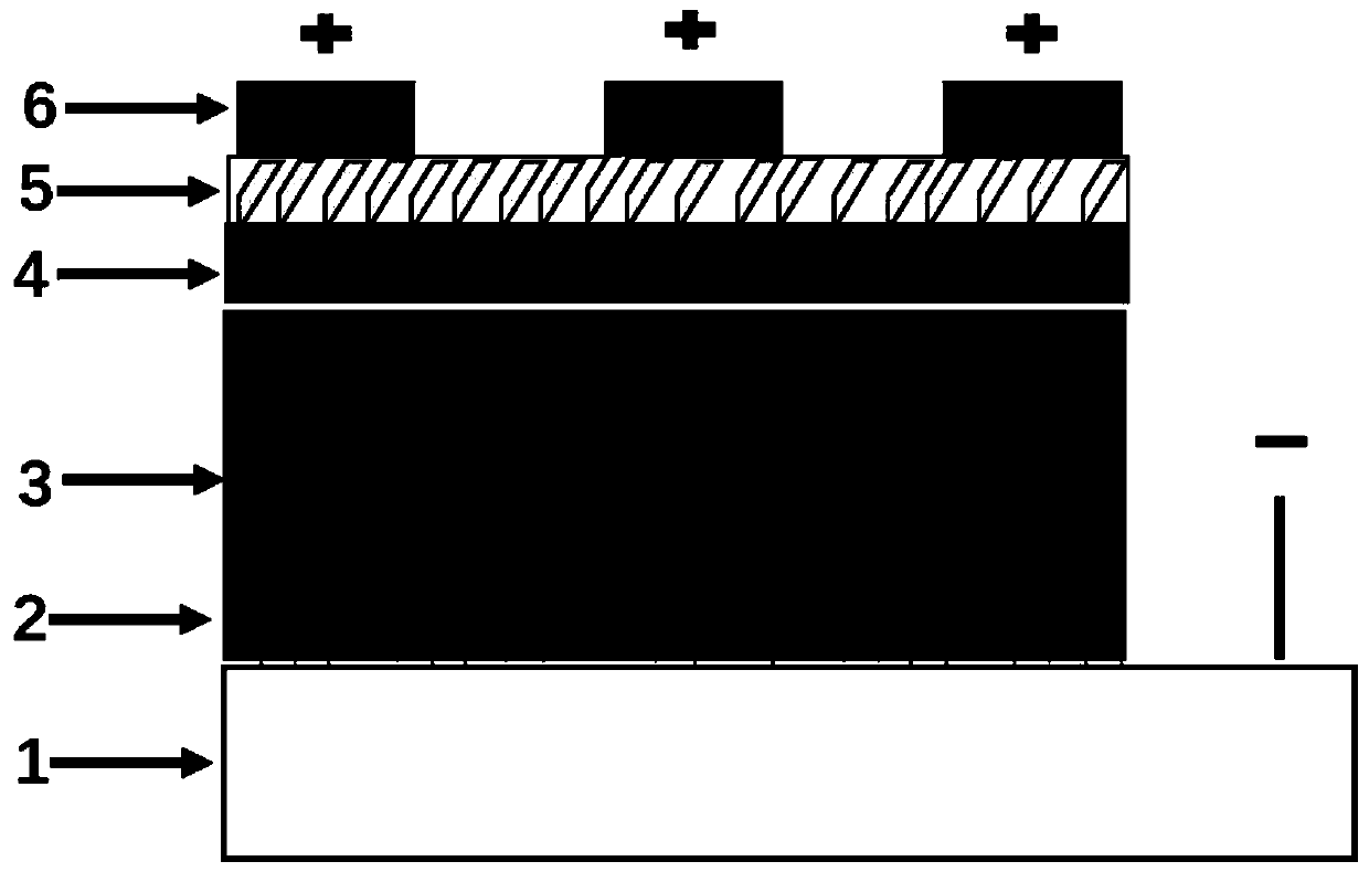
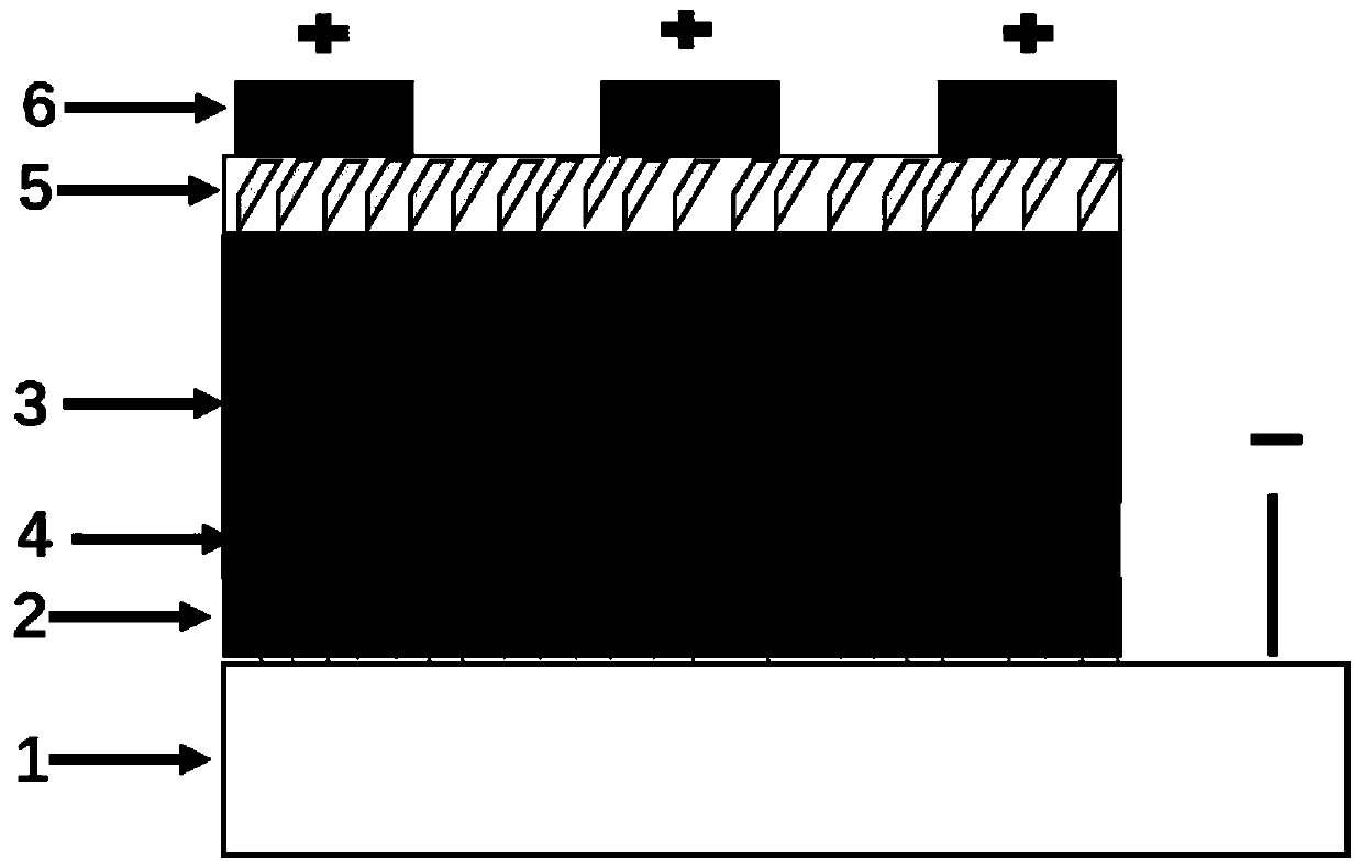
[0038] Such as figure 1 As shown, a planar structure perovskite photovoltaic cell includes a transparent conductive substrate, an electron transport layer, a perovskite photosensitive active layer, an interface passivation layer, a hole transport layer and a metal electrode, and its preparation method includes the following steps:
[0039] (1) Treatment of transparent conductive substrate: cleaning FTO (fluorine-doped SnO 2 ) conductive glass sheet, first soak the conductive glass sheet in a solution containing a cleaning agent (such as Libai brand liquid detergent) for 30 minutes, then repeatedly scrub and rinse with clean water; then polish with polishing powder; then respectively Put it into a vessel containing deionized water, acetone and alcohol and sonicate it for 20 minutes; finally put it in deionized water and rinse it twice, blow dry with a nitrogen gun and put it in an oven at 80°C for drying;
[0040] (2)SnO 2 Preparation of QD thin films: SnO on FTO substrates ...
Embodiment 2
[0052] Such as figure 1 As shown, a planar structure perovskite photovoltaic cell includes a transparent conductive substrate, an electron transport layer, a perovskite photosensitive active layer, an interface passivation layer, a hole transport layer and a metal electrode, and its preparation method includes the following steps:
[0053] (1) cleaning ITO conductive glass sheet: with embodiment 1;
[0054] (2)SnO 2 Thin Film Preparation: SnO Fabrication on ITO Substrates 2 film, and put it into a UV-ozone cleaner, and treat it with UV-ozone for 15 minutes in an atmospheric atmosphere and at room temperature, and the treated SnO 2 / ITO substrate is quickly transferred into the glove box;
[0055] (3) Preparation of perovskite photosensitive active layer: same as Example 1;
[0056] (4) Prepare an interface passivation layer on the perovskite photosensitive film:
[0057] a. Solution preparation: Dissolve the previously synthesized Au@CdS nanoparticles with a particle size...
Embodiment 3
[0063] Such as figure 1 As shown, a planar structure perovskite photovoltaic cell includes a transparent conductive substrate, an electron transport layer, a perovskite photosensitive active layer, an interface passivation layer, a hole transport layer and a metal electrode, and its preparation method includes the following steps:
[0064] (1) cleaning FTO conductive glass sheet: with embodiment 1;
[0065] (2)SnO 2 QD film preparation: with embodiment 1;
[0066] (3) Preparation of perovskite photosensitive active layer: same as Example 1;
[0067] (4) Prepare an interface passivation layer on the perovskite photosensitive film:
[0068]a. Solution preparation: Dissolve the previously synthesized Au@CdS nanoparticles with a particle size of 30nm and a CdS-wrapped thickness of 10nm in 1ml of chlorobenzene solvent, sonicate in an ultrasonic cleaner for 1h, and the solution concentration is 0.03mmol / mL. stand-by;
[0069] b. Preparation of interface passivation layer: In an...
PUM
 Abstract
Description
Claims
Application Information


