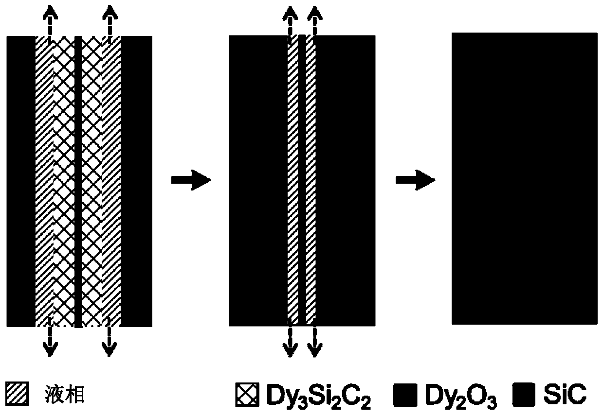
Connecting material for connecting silicon carbide material, and application thereof
A connection material, silicon carbide technology, applied in the connection of silicon carbide ceramics and its composite materials, silicon carbide and its composite materials, can solve the difficulty of direct connection, the difference in thermal and mechanical properties between the connection joint and the silicon carbide substrate, etc. Problems, to achieve the effect of densification sintering, lower temperature, and promote atomic diffusion
- Summary
- Abstract
- Description
- Claims
- Application Information
AI Technical Summary
Problems solved by technology
Method used
Image
Examples
Embodiment 1
[0058] In this embodiment, the material to be connected is silicon carbide ceramics, and the material of the connection layer is Dy 3 Si 2 C 2 Coating, Dy 3 Si 2 C 2 The XRD characterization of Figure 4a shown. The connection method is electric field assisted connection. The specific implementation steps are as follows:
[0059] (1) Roughly polish the surface of silicon carbide ceramics with a diameter of 20 mm and a height of 20 mm with a 5 μm diamond polishing solution to remove large defects and impurities on the surface;
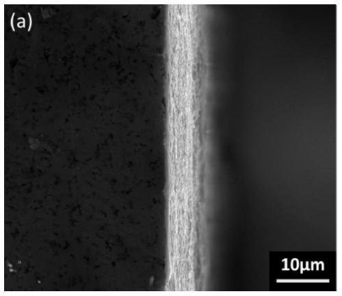
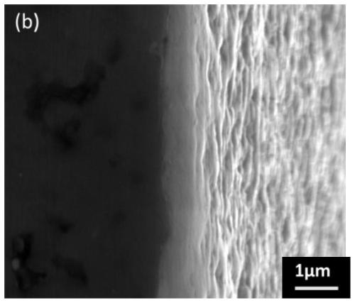
[0060] (2) Using the molten salt method, in a tube furnace at 900°C for 60 minutes, the rare earth dysprosium (Dy) reacts in situ on the surface of silicon carbide to form Dy with a thickness of about 1 μm 3 Si 2 C 2 coating, such as Figure 2a and Figure 2b shown;
[0061] (3) then the silicon carbide of two cladding coatings is packed in the graphite mold that diameter is 20mm;
[0062] (4) Place the graphite mold with the sample in the...
Embodiment 2
[0065] In this embodiment, the material to be connected is silicon carbide ceramics, and the material of the connection layer is Dy 3 Si 2 C 2 Coating, the connection method is electric field assisted connection. The specific implementation steps are as follows:
[0066] (1) Roughly polish the surface of silicon carbide ceramics with a diameter of 20 mm and a height of 20 mm with a 5 μm diamond polishing solution to remove large defects and impurities on the surface;
[0067] (2) Coating a Dy rare earth film with a thickness of 2000nm on the surface of silicon carbide by PVD method, and then heat treatment at 900°C to obtain Dy 3 Si 2 C 2 coating;
[0068] (3) then the silicon carbide of two cladding coatings is packed in the graphite mold that diameter is 20mm;
[0069] (4) Place the graphite mold with the sample in the spark plasma sintering furnace, pass the current, and raise the temperature to 1300°C, 1400°C, 1500°C, 1600°C at a rate of 100°C / min, keep it warm for ...
Embodiment 3
[0072] In this embodiment, the material to be connected is silicon carbide ceramics, and the material of the connection layer is Sm 3 Si 2 C 2 Coating, Sm 3 Si 2 C 2 The XRD characterization of Figure 4b As shown, the connection method is electric field assisted connection. The specific implementation steps are as follows:
[0073] (1) Roughly polish the surface of silicon carbide ceramics with a diameter of 20 mm and a height of 20 mm with a 5 μm diamond polishing solution to remove large defects and impurities on the surface;
[0074] (2) In situ preparation of Sm on SiC surface by molten salt method 3 Si 2 C 2 coating;
[0075] (3) Two pieces of coated silicon carbide are then installed in a graphite mold with a diameter of 20 mm.
[0076] (4) Place the graphite mold with the sample installed in the spark plasma sintering furnace, pass the current, and raise the temperature to 1300°C, 1400°C, 1500°C, 1600°C, 1700°C at a rate of 100°C / min, and keep it warm for 10...
PUM
| Property | Measurement | Unit |
|---|---|---|
| thickness | aaaaa | aaaaa |
| flexural strength | aaaaa | aaaaa |
| strength | aaaaa | aaaaa |
Abstract
Description
Claims
Application Information


