Semiconductor structure and formation method thereof

A semiconductor, regional technology, used in semiconductor devices, semiconductor/solid-state device manufacturing, electrical components, etc., to solve problems such as poor performance of multi-threshold voltage transistors

Active Publication Date: 2019-10-29
SEMICON MFG INT (SHANGHAI) CORP +1
View PDF20 Cites 3 Cited by
  • Summary
  • Abstract
  • Description
  • Claims
  • Application Information

AI Technical Summary

Problems solved by technology

[0005] However, the performance of multi-threshold

Method used


Image

  • Semiconductor structure and formation method thereof
  • Semiconductor structure and formation method thereof
  • Semiconductor structure and formation method thereof

Examples


Embodiment Construction

[0034] As mentioned in the background, the performance of the semiconductor structures formed by the prior art is poor.

[0035] Figure 1 to Figure 3 It is a structural schematic diagram of each step of a method for forming a semiconductor structure.

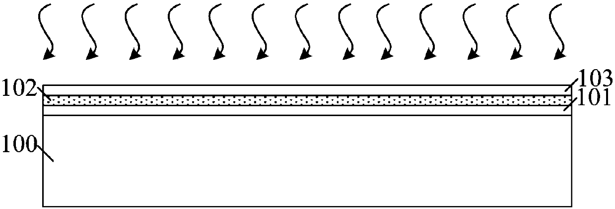
[0036] Please refer to figure 1 , providing a substrate 100; forming an interface layer 101 on the substrate 100; forming a gate dielectric layer 102 on the interface layer 101; forming a sacrificial layer 103 on the gate dielectric layer 102; forming the sacrificial layer 103 Afterwards, an annealing treatment is performed on the interface layer 101 and the gate dielectric layer 102 .

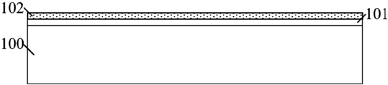
[0037] Please refer to figure 2 , after the annealing treatment, the sacrificial layer 103 is removed.

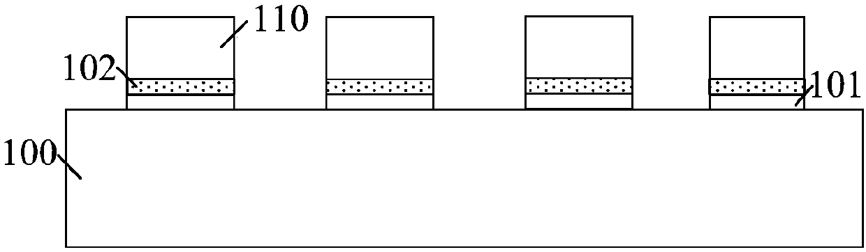
[0038] Please refer to image 3 After removing the sacrificial layer 103, a gate layer 110 is formed on the gate dielectric layer 102; a patterned mask layer is formed on the gate layer 110; The gate layer 110 , the gate dielectric la...


PUM

PropertyMeasurementUnit
Thicknessaaaaaaaaaa
Thicknessaaaaaaaaaa
Thicknessaaaaaaaaaa

Abstract

The invention discloses a semiconductor structure and a formation method thereof. The method includes providing a substrate, wherein the substrate includes a first area; forming a gate dielectric layer on the first area of the substrate; forming a protective layer on the gate dielectric layer of the first area, wherein the material of the protective layer is a non-crystalline material, and the protective layer has doped ions; and forming a grid electrode on the protective layer of the first area. The protective layer can be taken as a work function layer of the formed semiconductor structure,so that the protective layer cannot be removed in follow-up process, and therefore, technological process can be simplified; and the protective layer can be protected from damaging the gate dielectriclayer during removing, so that the performance of the formed semiconductor structure can be improved.

Description

technical field [0001] The invention relates to the field of semiconductor manufacturing, in particular to a semiconductor structure and a forming method thereof. Background technique [0002] With the continuous progress of semiconductor technology, the integration level of semiconductor devices has been continuously improved, which requires that more transistors can be formed on a chip. [0003] Threshold voltage is an important property of transistors and has a significant impact on transistor performance. Transistors with different functions often have different requirements on threshold voltages. During the process of forming different transistors, the threshold voltages of different transistors need to be adjusted. [0004] In order to adjust the threshold voltages of different transistors, a work function layer is formed on the surface of the gate dielectric layer of the transistors. The work function layer includes: a P-type work function layer and an N-type work f...

Claims


Application Information

Patent Timeline
IPC IPC(8): H01L29/06H01L21/336
CPCH01L29/66007H01L29/0657H01L29/06
Inventor 李勇
Owner SEMICON MFG INT (SHANGHAI) CORP
Why Eureka
Try Eureka