Vertical cavity surface emitting laser and manufacturing method thereof

A technology of vertical cavity surface emission and manufacturing method, which is applied in the field of vertical cavity surface emitting laser and its production, which can solve the problems of AlInP material oxidation, low threshold, and affecting output power, so as to reduce free carrier absorption and reduce difficulty , the effect of reducing resistance

Inactive Publication Date: 2019-11-08
INST OF SEMICONDUCTORS - CHINESE ACAD OF SCI
View PDF5 Cites 12 Cited by
  • Summary
  • Abstract
  • Description
  • Claims
  • Application Information

AI Technical Summary

Problems solved by technology

[0004] Due to gallium arsenide (GaAs) absorption problem (at 940nm band, p-type doping is 1.6*10 19 /cm -3 The absorption coefficient is 100cm -1 ), based on the AlGaAs/GaAs material system, people made a suspended AlGaAs-based HCG, which replaced part of the upper DBR of the VCSEL in the 850nm band, and realized single-mode, single-polarization, low threshold, and fast wavelength tunable work, but AlGaAs is p-type Doping, there is a s

Method used


Image

  • Vertical cavity surface emitting laser and manufacturing method thereof
  • Vertical cavity surface emitting laser and manufacturing method thereof
  • Vertical cavity surface emitting laser and manufacturing method thereof

Examples


Embodiment 1

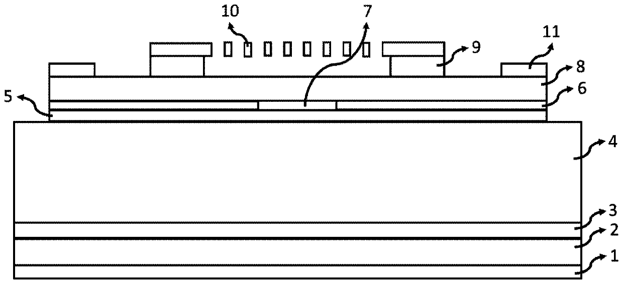
[0070] Embodiment 1 of the present invention provides a vertical cavity surface emitting laser. figure 1 It is a schematic structural diagram of a vertical cavity surface emitting laser according to Embodiment 1 of the present invention; Figure 4 It is a scanning electron microscope image of the suspended GaAs-based HCG layer in Example 1 of the present invention. Such as figure 1 with Figure 4 As shown, the vertical cavity surface emitting laser of the present invention has an operating wavelength of 940nm, including a substrate 2, a buffer layer 3, a lower DBR4, an active layer 5, a current confinement layer 6, a current confinement aperture 7, and a current diffusion layer 8. GaInP sacrificial layer 9 , non-doped suspension type GaAs-based HCG layer 10 , n-side electrode 1 and p-side electrode 11 .

[0071] Substrate 2 is an n-type GaAs substrate.

[0072] The buffer layer 3 is n-type GaAs.

[0073] Lower DBR4 is n-type Al 0.12 Ga 0.88 As / Al 0.9 Ga 0.1 As is DBR....

Embodiment 2

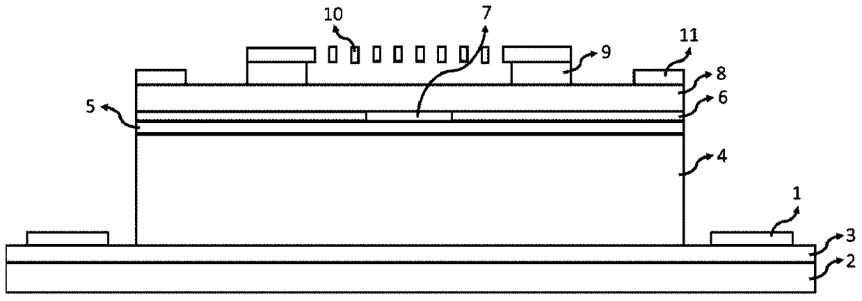
[0092] Embodiment 2 of the present invention provides a vertical cavity surface emitting laser, figure 2 It is a schematic structural diagram of a vertical cavity surface emitting laser according to Embodiment 2 of the present invention; Figure 4 It is a scanning electron microscope image of the suspended GaAs-based HCG layer in Example 2 of the present invention. Such as figure 2 with Figure 4 As shown, the vertical cavity surface emitting laser of the present invention has an operating wavelength of 980nm, including a substrate 2, a buffer layer 3, a lower DBR4, an active layer 5, a current confinement layer 6, a current confinement aperture 7, and a current diffusion layer 8, GaInP sacrificial layer 9 , non-doped suspension type GaAs-based HCG layer 10 , n-side electrode 1 , and p-side electrode 11 .

[0093] Substrate 2 is an n-type GaAs substrate.

[0094] The buffer layer 3 is n-type GaAs.

[0095] Lower DBR4 is n-type Al 0.12 Ga 0.88 As / Al 0.9 Ga 0.1 As is ...

Embodiment 3

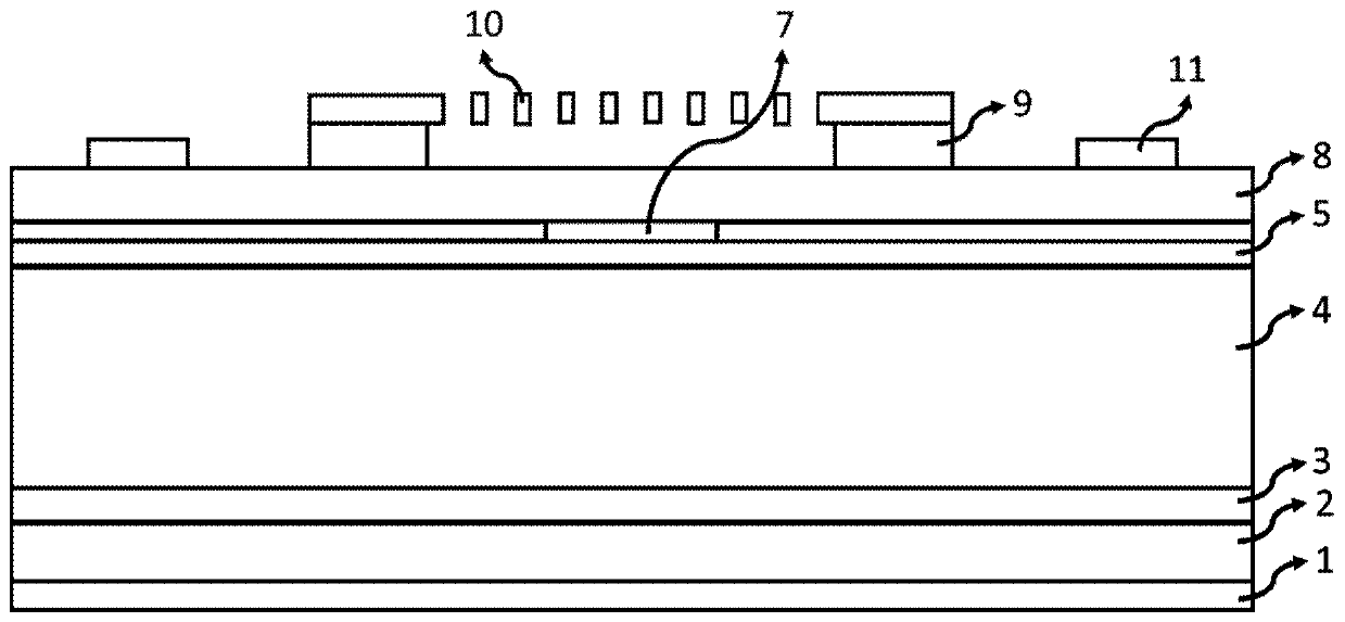
[0115] Embodiment 3 of the present invention provides a vertical cavity surface emitting laser, image 3 It is a schematic structural diagram of a vertical cavity surface emitting laser according to Embodiment 3 of the present invention. Such as image 3 As shown, the vertical cavity surface emitting laser of the present invention has an operating wavelength of 1550nm, including a substrate 2, a buffer layer 3, a lower DBR4, an active layer 5, a current confinement aperture 7, a current diffusion layer 8, and an InGaAs sacrificial layer 9, Non-doped suspension type InP-based HCG layer 10 , n-side electrode 1 , and p-side electrode 11 .

[0116] Substrate 2 is an n-type InP substrate.

[0117] The buffer layer 3 is n-type InP.

[0118] The lower DBR4 is an n-type InGaAlAs / InAlAs-based DBR.

[0119] The active layer 5 is three InGaAlAs quantum wells.

[0120] The current confining aperture 7 consists of a tunnel structure.

[0121] The current spreading layer 8 is n-type I...


PUM


Abstract

The present invention provides a vertical cavity surface emitting laser and a manufacturing method thereof. The vertical cavity surface emitting laser comprises a substrate, a buffer layer, a lower DBR, an active layer, a current limiting aperture, a current diffusion layer, an undoped suspension type HCG layer, an n side electrode and a p-side electrode. The material extension difficulty of the vertical cavity surface emitting laser is reduced, the universality of material growth is improved, the free carrier absorption is reduced, and the output efficiency of the device is improved; and thevertical cavity surface emitting laser has polarization selection and single mode output characteristics, and can be expanded to a tunable vertical cavity surface emitting laser. The vertical cavity surface emitting laser can be applied to the fields such as optical communication, optical interconnection, optical sensing, medical imaging and the like.

Description

technical field [0001] The invention relates to the technical field of semiconductor optoelectronic devices, in particular to a vertical cavity surface emitting laser and a manufacturing method thereof. Background technique [0002] A vertical cavity surface emitting laser (VCSEL) is composed of a substrate, a lower Bragg reflector, an active region, an oxide layer, an upper Bragg reflector, a positive electrode and a negative electrode, etc. Composed of a Bragg reflector (DBR), the laser is output along the material growth direction, that is, perpendicular to the substrate. Due to the unique device structure of VCSEL, it has the advantages of low power consumption, fast modulation speed, small size, low cost, high reliability, circular beam, and two-dimensional array integration. It is widely used in optical communication, optical interconnection, printing, Display, sensing, consumer electronics and other fields. [0003] The distributed Bragg reflector (DBR) is composed ...

Claims


Application Information

Patent Timeline
IPC IPC(8): H01S5/183H01S5/187H01S5/042
CPCH01S5/0425H01S5/18308H01S5/18361H01S5/187H01S2304/00
Inventor 刘安金杨礴
Owner INST OF SEMICONDUCTORS - CHINESE ACAD OF SCI
Why Eureka
Try Eureka