Groove-digging preparation method for thick-film silicon nitride waveguide

A silicon nitride and waveguide technology, applied in the field of integrated optics, can solve the problems of insufficiently steep sidewalls, large waveguide losses, and rough sidewalls, so as to avoid unevenness, reduce waveguide losses, and reduce sidewall roughness. Effect

Active Publication Date: 2019-11-12
INST OF MICROELECTRONICS CHINESE ACAD OF SCI
View PDF6 Cites 6 Cited by
  • Summary
  • Abstract
  • Description
  • Claims
  • Application Information

AI Technical Summary

Problems solved by technology

[0003] In order to overcome the technical problems of high stress in the thick film of silicon nitride deposition in the prior art, the side wall is not steep enough, the side wall is rough, and the waveguide loss is large, and a method for preparing a trench for thick film silicon nitride waveguide is provided. To meet different design needs

Method used


Image

  • Groove-digging preparation method for thick-film silicon nitride waveguide
  • Groove-digging preparation method for thick-film silicon nitride waveguide
  • Groove-digging preparation method for thick-film silicon nitride waveguide

Examples


preparation example Construction

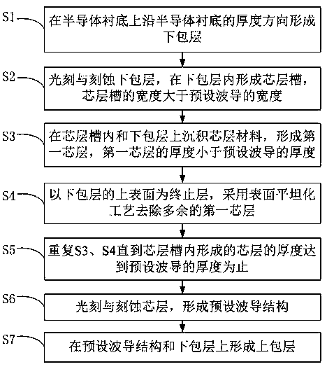
[0026] In this embodiment, a method for preparing grooves of a thick-film silicon nitride waveguide, such as figure 1 shown, including:

[0027] S1. Forming a lower cladding layer on the semiconductor substrate along the thickness direction of the semiconductor substrate;

[0028] On the basis of the above solutions, further, the semiconductor substrate in this implementation manner is a silicon substrate, and in other implementation manners, the semiconductor substrate may also be a quartz substrate.

[0029] On the basis of the above solution, further, the lower cladding layer is formed by thermal oxidation and / or chemical vapor deposition process, and in other embodiments, the lower cladding layer can also be formed by physical vapor deposition process. The lower cladding material includes a solid cladding material with a refractive index lower than 1.7 and higher than 1, preferably silicon dioxide.

[0030] S2. Photolithography and etching the lower cladding layer to for...


PUM

PropertyMeasurementUnit
thicknessaaaaaaaaaa
widthaaaaaaaaaa
widthaaaaaaaaaa

Abstract

The invention discloses a groove-digging preparation method for a thick-film silicon nitride waveguide. The preparation method comprises the following steps: forming a lower cladding on a semiconductor substrate in a thickness direction of the semiconductor substrate; photoetching and etching the lower cladding, and forming a core layer groove in the lower cladding, wherein the core layer groove is wider than a preset waveguide; depositing a core layer material in the core layer groove and on the lower cladding, thus forming a first core layer, wherein the first core layer is thinner than thepreset waveguide; taking the upper surface of the lower cladding as a stop layer, and removing redundant first core layer by adopting a surface planarization technology; repeating the steps until thethickness of the core layer formed in the core layer groove reaches the thickness of the preset waveguide; photoetching and etching the core layer, thus forming a preset waveguide structure; and forming an upper cladding on the preset waveguide structure and the lower cladding. The scheme of the invention solves a high stress problem caused by a thin film which is too thick; meanwhile, shape of the waveguide is optimized, roughness of the side wall is reduced, steep degree of the waveguide is increased, and loss of the waveguide is reduced.

Description

technical field [0001] The invention relates to the technical field of integrated optics, in particular to a method for preparing grooves for a thick-film silicon nitride waveguide. Background technique [0002] At present, the silicon nitride film growth preparation methods mainly include plasma chemical vapor deposition (PECVD) and low pressure chemical vapor deposition (LPCVD). Among them, the silicon nitride film deposited by low-pressure chemical vapor deposition (LPCVD) has better quality and lower waveguide loss. However, when the thickness of the film is greater than 300 nanometers, due to the difference in thermal expansion coefficient between the film and the substrate, when the film grows in a large area, there will be a large stress and cracks will easily occur, thereby affecting the performance of the device. In the existing production process, a dry etching process is usually used to open a groove in the silicon dioxide cladding layer, and then fill the groove...

Claims


Application Information

Patent Timeline
Patent Type & Authority Applications(China)
IPC IPC(8): G02B6/136G02B6/138
CPCG02B6/136G02B6/138
Inventor 李彬李志华刘若男
Owner INST OF MICROELECTRONICS CHINESE ACAD OF SCI
Why Eureka
Try Eureka