High electron mobility transistor and preparation method thereof

A high electron mobility, transistor technology, applied in transistors, semiconductor/solid-state device manufacturing, circuits, etc., can solve problems affecting the quality of GaN crystals, destroying the GaN crystal structure, affecting the performance of high electron mobility transistors, etc., to achieve the suppression of Si Diffusion into GaN improves crystal quality and improves performance

Active Publication Date: 2019-11-12
HC SEMITEK ZHEJIANG CO LTD
View PDF6 Cites 2 Cited by
  • Summary
  • Abstract
  • Description
  • Claims
  • Application Information

AI Technical Summary

Problems solved by technology

[0005] When GaN is directly grown on a Si substrate, the substrate Si will react with the N source introduced during the epitaxial growth process to form amorphous SiN, which affects the crystal quality of GaN, and even diffuses into GaN, destroying the crystal of GaN structure, which seriously affects the performance of high electron mobility transistors

Method used


Image

  • High electron mobility transistor and preparation method thereof
  • High electron mobility transistor and preparation method thereof
  • High electron mobility transistor and preparation method thereof

Examples


Embodiment Construction

[0032] In order to make the object, technical solution and advantages of the present invention clearer, the implementation manner of the present invention will be further described in detail below in conjunction with the accompanying drawings.

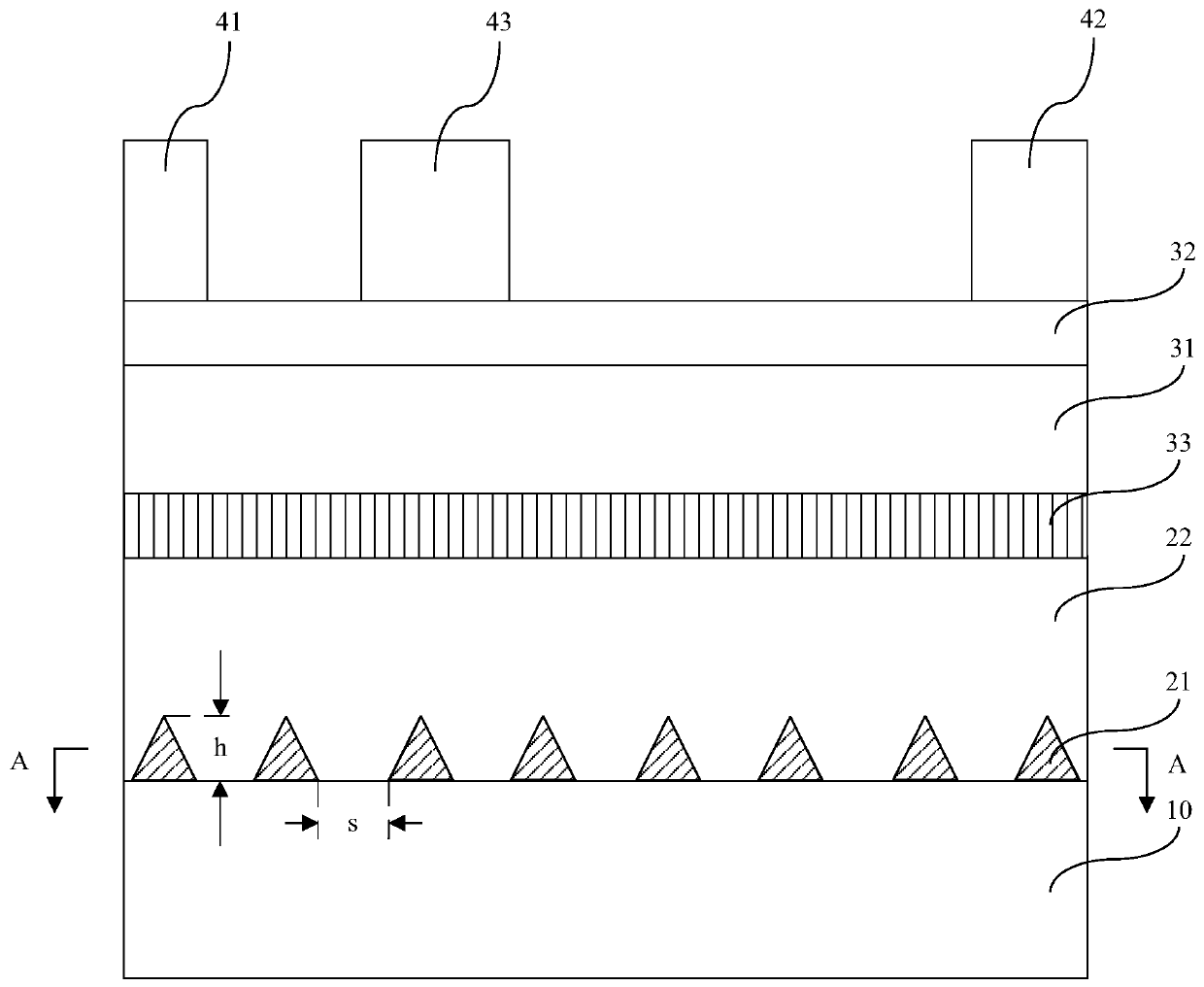
[0033] An embodiment of the present invention provides a high electron mobility transistor. figure 1 A schematic structural diagram of a high electron mobility transistor provided by an embodiment of the present invention. see figure 1 , the high electron mobility transistor includes a Si substrate 10 , a plurality of AlN seeds 21 , an AlN buffer layer 22 , a GaN channel layer 31 , an AlGaN barrier layer 32 , a source 41 , a drain 42 and a gate 43 .

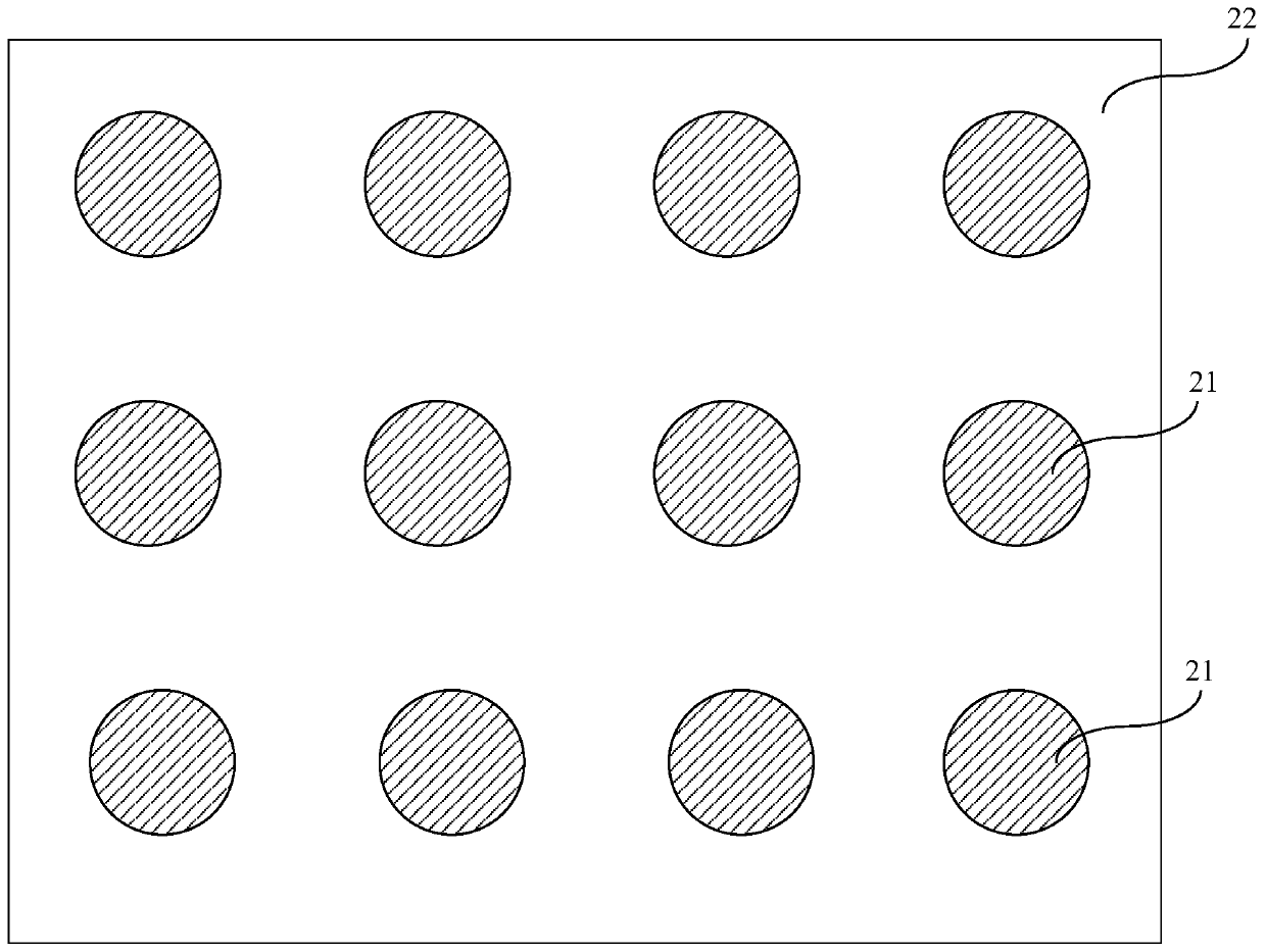
[0034] figure 2 Provided for the embodiment of the present invention figure 1 Sectional view along A-A direction. see figure 2 and figure 1 , a plurality of AlN crystal seeds 21 are evenly distributed on the first surface 100 of the Si substrate 10, an AlN buffer layer 22 is dispo...


PUM


Abstract

The invention discloses a high electron mobility transistor and a preparation method thereof, and belongs to the technical field of semiconductors. The high electron mobility transistor comprises a Sisubstrate, a plurality of AlN seed crystals, AlN buffer layers, a GaN channel layer, an AlGaN barrier layer, a source electrode, a drain electrode and a grid electrode; the multiple AlN crystal seedsare uniformly distributed on the first surface of the Si substrate; the AlN buffer layer is arranged on the AlN seed crystals and fills the space among the AlN seed crystals, and the AlN buffer layers on the respective AlN crystal seeds have the same crystal orientation; the GaN channel layer and the AlGaN barrier layer are sequentially stacked on the second surface of the AlN buffer layer, and the second surface is a plane; the source electrode, the drain electrode and the grid electrode are arranged on the AlGaN barrier layer separately, the source electrode and the drain electrode are in ohmic contact with the AlGaN barrier layer; and the grid electrode and the AlGaN barrier layer form schottky contact. According to the transistor, the crystal quality of the GaN channel layer can be improved.

Description

technical field [0001] The invention relates to the technical field of semiconductors, in particular to a high electron mobility transistor and a preparation method thereof. Background technique [0002] A high electron mobility transistor (English: High electron mobility transistor, HEMT for short) is a type of field effect transistor, which uses two materials with different energy gaps to form a heterojunction to provide a channel for carriers. Gallium nitride (GaN)-based materials have the characteristics of wide band gap, high electron mobility, high voltage resistance, radiation resistance, easy formation of heterostructures, and large spontaneous polarization effect, and are suitable for the preparation of new generation high-frequency high-power microelectronic devices such as HEMTs and circuits. [0003] Existing high electron mobility transistors include a substrate, a channel layer, a barrier layer, a source, a drain, and a gate. The channel layer and the barrier ...

Claims


Application Information

Patent Timeline
Patent Type & Authority Applications(China)
IPC IPC(8): H01L29/778H01L29/10H01L21/335
CPCH01L29/7786H01L29/1075H01L29/66462Y02P70/50
Inventor 洪威威王倩周飚胡加辉
Owner HC SEMITEK ZHEJIANG CO LTD
Why Eureka
Try Eureka