
Lateral insulated gate bipolar transistor and preparation method thereof

A bipolar transistor, insulated gate technology, applied in semiconductor/solid-state device manufacturing, semiconductor devices, electrical components, etc., can solve the problems of weak conductance modulation effect in the drift region, high forward voltage drop, slow turn-off speed, etc. Achieve the effect of optimizing carrier distribution, reducing forward conduction voltage drop, and reducing driving loss

Active Publication Date: 2019-11-15
UNIV OF ELECTRONIC SCI & TECH OF CHINA
View PDF15 Cites 1 Cited by
  • Summary
  • Abstract
  • Description
  • Claims
  • Application Information

AI Technical Summary

Problems solved by technology

When the device is in forward conduction, the holes injected by the collector junction enter the drift region, and since the minority carriers in the drift region flow away from the base region, the conductance modulation effect in the drift region is weak, and the forward conduction voltage drop is high; and Due to the large injection effect, the turn-off speed of the device is slow when it is turned off, and there is a serious current tailing phenomenon, which will cause a large turn-off loss in use, so the turn-on voltage drop and turn-off loss of the traditional lateral IGBT device Medium characteristics are poor

Method used


Image

  • Lateral insulated gate bipolar transistor and preparation method thereof
  • Lateral insulated gate bipolar transistor and preparation method thereof
  • Lateral insulated gate bipolar transistor and preparation method thereof

Examples


Embodiment 1

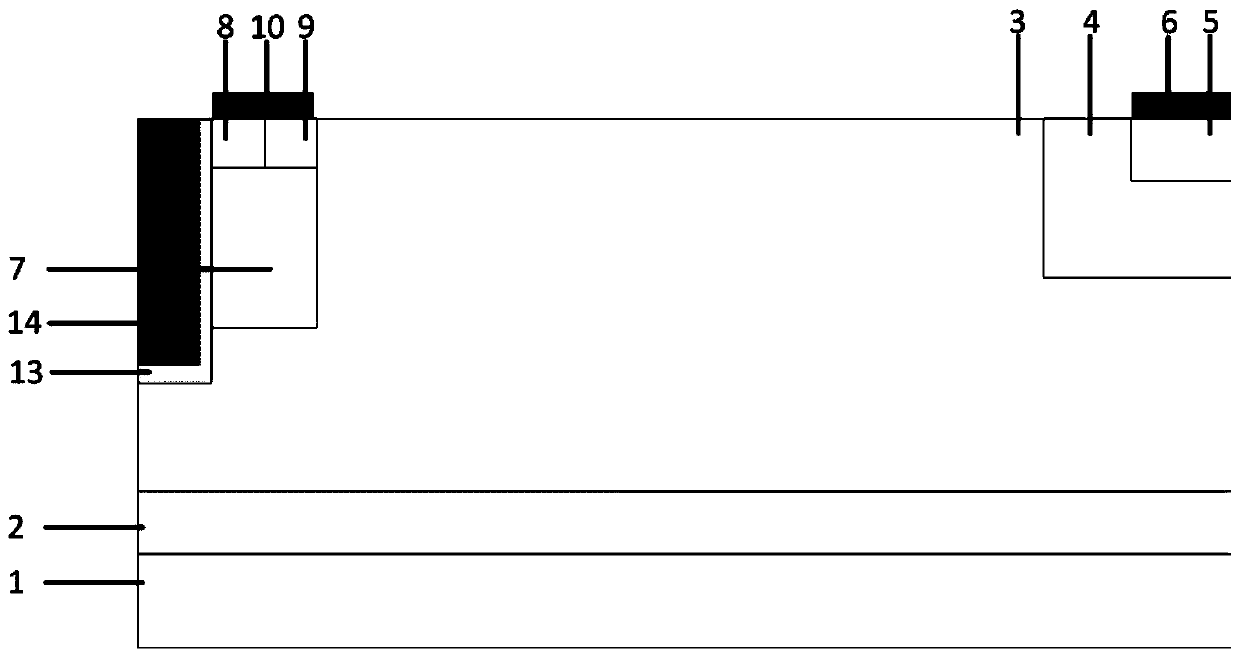
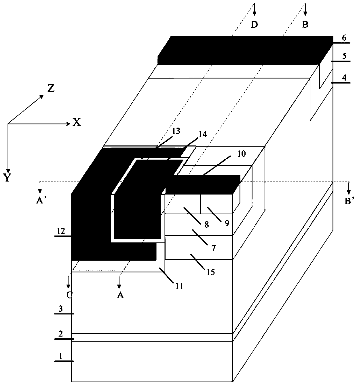
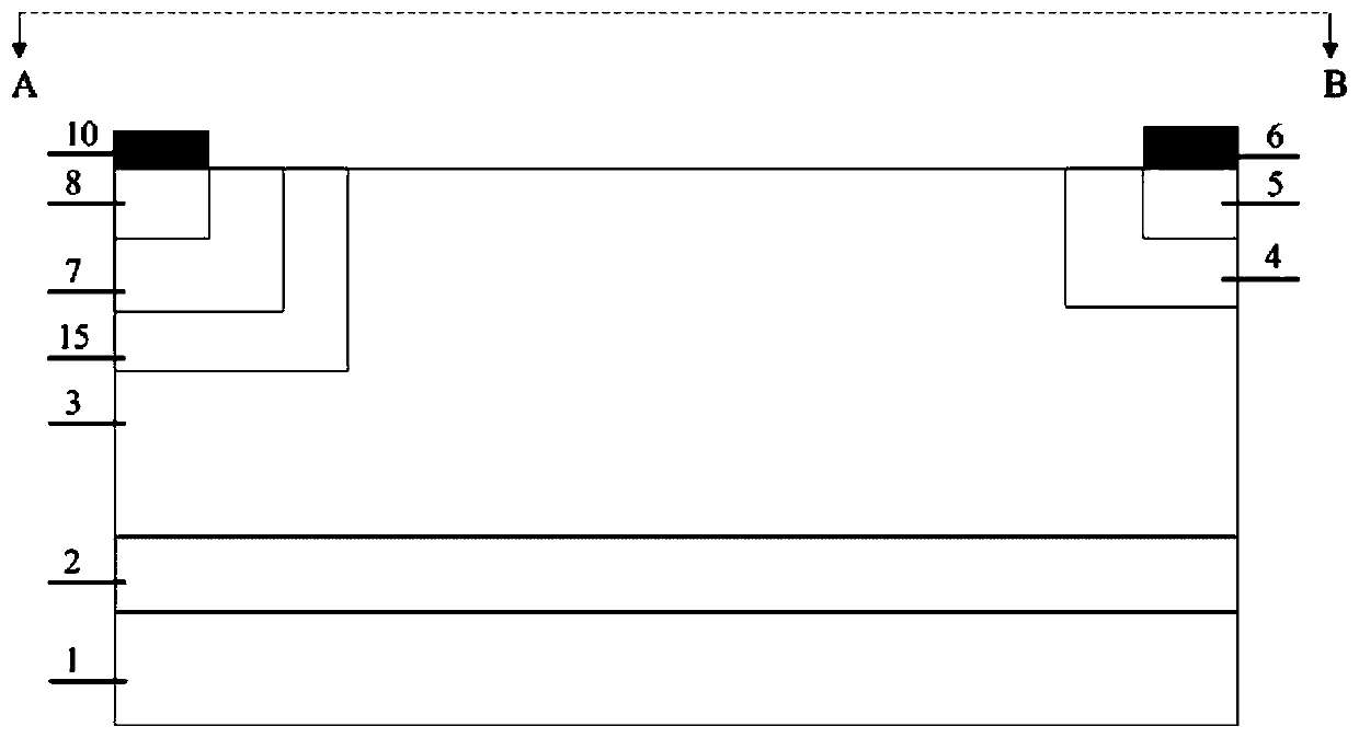
[0059] This embodiment provides a lateral insulated gate bipolar transistor, the half-cell structure of which is as follows figure 2 As shown, the two-dimensional cross-sectional structures obtained along the dotted line AB and dotted line CD in the semi-cellular structure are as follows image 3 and Figure 4 shown. This embodiment includes a P-type substrate 1, a silicon dioxide isolation layer 2, and an N-type drift region 3 arranged in sequence from bottom to top; an N-type buffer zone 4 is arranged on one side of the top layer of the N-type drift region 3 in the longitudinal direction, so The longitudinal direction is the third dimension perpendicular to the horizontal and vertical directions of the device; the N-type buffer zone 4 is provided with an N-type collector region 5, and the upper surface of the N-type collector region 5 is provided with a first metallized collector 6; In the N-type drift region 3, a P-type base region 7 is provided on the side away from the...

Embodiment 2

[0066] This embodiment provides a lateral insulated gate bipolar transistor, the half-cell structure of which is as follows Figure 5 As shown, its two-dimensional cross-sectional view along the dotted line AB in the figure is as follows Figure 6 shown. In this embodiment, on the basis of Embodiment 1, in the first trench gate structure, the vertical direction below the first silicon dioxide layer 11 and the longitudinal direction of the N-type drift region 3 are close to the side of the first silicon dioxide layer 1 A P-type shielding layer 16 is provided, and the doping concentration of the P-type shielding layer 16 is higher than that of the N-type drift region 3; a third gate oxide layer 131 is provided on the upper surface of the P-type base region 8, and the third gate oxide The layer 131 extends vertically above the N-type charge storage region 15 ; a second polysilicon gate electrode 141 is disposed above the third gate oxide layer 131 .

[0067] In particular, the ...

Embodiment 3

[0071] This embodiment provides a lateral insulated gate bipolar transistor, the cell structure of which is as follows Figure 7 As shown, on the basis of Embodiment 1, the polysilicon gate electrode 14 and the second silicon dioxide layer 13 in the longitudinal direction length greater than the N-type emitter region 8 longitudinal direction length of the part toward the N-type emitter region 8 in the horizontal direction The direction extends until the cell boundary.

[0072] In particular, the longitudinal border of the N-type charge storage region 15 coincides with the longitudinal outer border of the second silicon dioxide layer 13 .

[0073] Compared with Example 1, the extended gate is between the collector and the emitter, which can block the flow of carriers during conduction, generate a carrier storage effect, improve the conductance modulation capability of the drift region, and reduce the conduction voltage drop ; At the same time, during forward conduction, the po...


PUM

PropertyMeasurementUnit
Thicknessaaaaaaaaaa

Abstract

The invention belongs to the technical field of power semiconductor devices and relates to a lateral insulated gate bipolar transistor and a manufacturing method thereof. Based on an LIGBT device structure, a carrier storage layer is added, the conductivity modulation effect in a drift region is enhanced, and the on-state voltage drop of a device is reduced. A grid electrode is wrapped with a separation gate, the Miller capacitance is reduced, the turn-off is reduced, the turn-off loss is reduced, and the compromise between a forward turn-on voltage drop (Vceon) and a turn-off loss (Eoff) is improved. The grid charge of the device can be reduced, the requirement for driving circuit ability is reduced, the driving loss is reduced, and the compromise characteristic between a current decreaserate (di / dt) and a turn-on loss (Eon) is optimized. A thick oxide layer at the bottom of a trench gate can reduce an electric field at a corner of a trench, the concentration of the electric field ata sharp corner of a bottom of the trench is alleviated, the breakdown voltage of the device is increased, the reliability of the device is improved, a thin gate oxide layer can reduce the threshold voltage of the device, and the latch current density can be increased.

Description

technical field [0001] The invention belongs to the technical field of power semiconductors, and in particular relates to a lateral insulated gate bipolar transistor. Background technique [0002] The lateral IGBT device is a horizontally integrated power device developed on the basis of the IGBT. It combines the advantages of the IGBT device structure, such as high input impedance, low driving power, reduced conduction voltage, fast switching speed, and strong voltage blocking capability. And it has obtained important applications in the field of horizontally integrated devices. [0003] As the feature size of semiconductor devices continues to decrease, the interaction between PN junctions inside the device and between devices through the substrate is becoming more and more serious, which greatly reduces the reliability of devices produced by traditional bulk silicon processes. SOI technology uses a buried oxide layer to isolate the top-layer silicon from the underlying s...

Claims


Application Information

Patent Timeline
IPC IPC(8): H01L29/06H01L29/423H01L29/739H01L21/28H01L21/331
CPCH01L29/7394H01L29/66325H01L29/0684H01L29/42312H01L29/401H01L29/0611
Inventor 张金平赵阳王康刘竞秀李泽宏张波
Owner UNIV OF ELECTRONIC SCI & TECH OF CHINA
Features
  • Generate Ideas
  • Intellectual Property
  • Life Sciences
  • Materials
  • Tech Scout
  • Unparalleled Data Quality
  • Higher Quality Content
  • 60% Fewer Hallucinations
Learn More