Preparation method of PERC battery as well as double-faced selective emitter PERC battery

An emitter, selective technology, applied in circuits, electrical components, climate sustainability, etc., can solve problems such as the inability to achieve good double-sided battery back printing, poor product results, and inability to achieve mass production. The cost of equipment and materials is limited, the yield is high, and the effect of improving quality

Inactive Publication Date: 2019-11-26
HANWHA SOLARONE QIDONG
View PDF6 Cites 10 Cited by
  • Summary
  • Abstract
  • Description
  • Claims
  • Application Information

AI Technical Summary

Problems solved by technology

The local boron doping process on the back is more difficult to control. The traditional technology generally achieves local back doping by opening a window on the passivation layer and printing boron paste, and then propelling it through high-temperature diffusion. Such a process is not only cumbersome, but also repeatedly The high temperature will also cause more lattice damage. In addition, due to the poor precision, the backside overprint of the double-sided battery cannot be well realized.
In view of the above shortcomings, those skilled in the art have studied the use of laser doping on the back of the silicon wafer, but the products obtained by the existing preparation process are not good, the yield is low, and mass production cannot be realized, so there is currently no way to realize the back of the silicon wafer. Selective Emitter PERC Cell Products with Local Doping

Method used


Image

  • Preparation method of PERC battery as well as double-faced selective emitter PERC battery
  • Preparation method of PERC battery as well as double-faced selective emitter PERC battery
  • Preparation method of PERC battery as well as double-faced selective emitter PERC battery

Examples


Embodiment 1

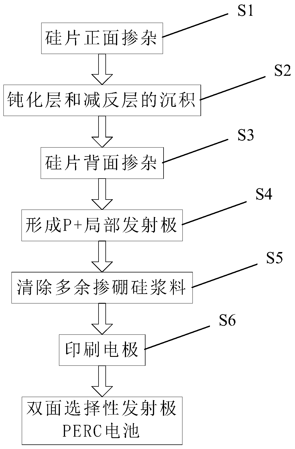
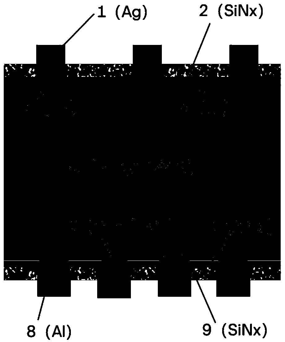
[0040] Such as figure 1 As shown, a method for preparing a double-sided selective emitter PERC battery in this embodiment includes the following steps:

[0041] Step S1: Front side doping of silicon wafer

[0042] Select P-type monocrystalline silicon wafers, first perform pre-cleaning and surface texturing, and then use low-pressure or normal-pressure diffusion furnaces to lightly dope phosphorus elements on the front to form N+ lightly doped regions. The doping concentration of N+ lightly doped regions is 3*E+20 / cm 3 , The square resistance is 120Ω / port.

[0043] The laser is used to heavily dope the front side of the silicon wafer to form a local N++ heavily doped region, and the doping concentration of the N++ heavily doped region is 2*E+20 / cm 3 , The sheet resistance is 70Ω / port.

[0044]The parameters of the laser in this step are as follows: the laser is a 532nm green laser, the laser power is 30W, the laser frequency is 250KHz, the laser running speed is 13m / s, and...

Embodiment 2

[0064] Such as figure 1 As shown, a method for preparing a double-sided selective emitter PERC battery in this embodiment includes the following steps:

[0065] Step S1: Front side doping of silicon wafer

[0066] Select P-type monocrystalline silicon wafers, first perform pre-cleaning and surface texturing, and then use a low-pressure or normal-pressure diffusion furnace to lightly dope phosphorus elements on the front to form an N+ lightly doped region. The doping concentration of the N+ lightly doped region is 1*E+20 / cm 3 , The square resistance is 110Ω / port.

[0067] The laser is used to heavily dope the front side of the silicon wafer to form a local N++ heavily doped region, and the doping concentration of the N++ heavily doped region is 2*E+20 / cm 3 , The square resistance is 50Ω / port.

[0068] The parameters of the laser in this step are as follows: the laser is a 532nm green laser, the laser power is 25W, the laser frequency is 200KHz, the laser running speed is 10...

Embodiment 3

[0088] Such as figure 1 As shown, a method for preparing a double-sided selective emitter PERC battery in this embodiment includes the following steps:

[0089] Step S1: Front side doping of silicon wafer

[0090] Select P-type monocrystalline silicon wafers, first perform pre-cleaning and surface texturing, and then use a low-pressure or normal-pressure diffusion furnace to lightly dope phosphorus elements on the front to form an N+ lightly doped region. The doping concentration of the N+ lightly doped region is 6*E+20 / cm 3 , The square resistance is 140Ω / port.

[0091] The laser is used to heavily dope the front side of the silicon wafer to form a local N++ heavily doped region, and the doping concentration of the N++ heavily doped region is 4*E+20 / cm 3 , The square resistance is 80Ω / port.

[0092] The parameters of the laser in this step are as follows: the laser is a 532nm green laser, the laser power is 40W, the laser frequency is 300KHz, the laser running speed is 15...


PUM


Abstract

The invention discloses a preparation method of a double-faced selective emitter PERC battery. The preparation method comprises the steps of doping the front of a textured P type silicon wafer and then completing deposition of a back passivation layer, a back antireflection layer, a front passivation layer and a front antireflection layer; the preparation method is characterized by also comprisingthe following steps: printing boron-silicon-doped slurry on the back passivation layer of the silicon wafer and drying, and then driving boron into a silicon substrate of the silicon wafer by adopting lasers in a region where the slurry is printed, thus a P+ emitter is formed; meanwhile, forming a linear open window, eliminating redundant boron-silicon-doped slurry by adopting a cleaning fluid and then performing secondary drying, printing front and back electrode slurry on the silicon wafer, and performing high temperature sintering, thus forming an electrode. The preparation method disclosed by the invention adds a drying step after boron slurry is printed, so that laser alignment accuracy is further improved, and product quality is improved; and a step of cleaning and removing the redundant boron-silicon-doped slurry after use of the lasers, so that local ohmic contact quality is improved.

Description

technical field [0001] The invention relates to the technical field of solar cell manufacturing, in particular to a preparation method of a double-sided selective emitter PERC battery and a double-sided selective emitter PERC battery prepared by the preparation method. Background technique [0002] Solar photovoltaic power generation, due to its clean, safe, convenient and high-efficiency characteristics, has become an emerging industry that is widely concerned and focused on development all over the world. [0003] As the thickness of the silicon wafer becomes lower and lower, the cost will be lower and lower, and at the same time, it will bring some negative effects. On the one hand, it will make it easier for minority carriers to diffuse to the surface of the silicon wafer to form recombination. On the other hand, it will cause some long-wave diffraction and transmission. Over the silicon wafer, resulting in a decrease in the conversion efficiency of the battery. Therefo...

Claims


Application Information

Patent Timeline
Patent Type & Authority Applications(China)
IPC IPC(8): H01L31/0216H01L31/18
CPCH01L31/02167H01L31/02168H01L31/18H01L31/1868Y02P70/50
Inventor 费存勇赵福祥崔钟亨
Owner HANWHA SOLARONE QIDONG
Why Eureka
Try Eureka