Thin film transistor and manufacturing method thereof

A technology of thin-film transistors and bottom gates, which is applied in transistors, semiconductor/solid-state device manufacturing, electric solid-state devices, etc., to achieve the effects of improving panel PPI, high electron mobility, device stability, and reducing device footprint

Pending Publication Date: 2019-12-03
FUJIAN HUAJIACAI CO LTD
View PDF0 Cites 5 Cited by
  • Summary
  • Abstract
  • Description
  • Claims
  • Application Information

AI Technical Summary

Problems solved by technology

The vertical structure TFT can reduce the device area, but the electron mobility and device stability of the structure still need to be further improved in terms of the existing process debugging

Method used


Image

  • Thin film transistor and manufacturing method thereof
  • Thin film transistor and manufacturing method thereof
  • Thin film transistor and manufacturing method thereof

Examples


Embodiment Construction

[0023] In order to explain in detail the technical content, structural features, achieved goals and effects of the technical solution, the following will be described in detail in conjunction with specific embodiments and accompanying drawings.

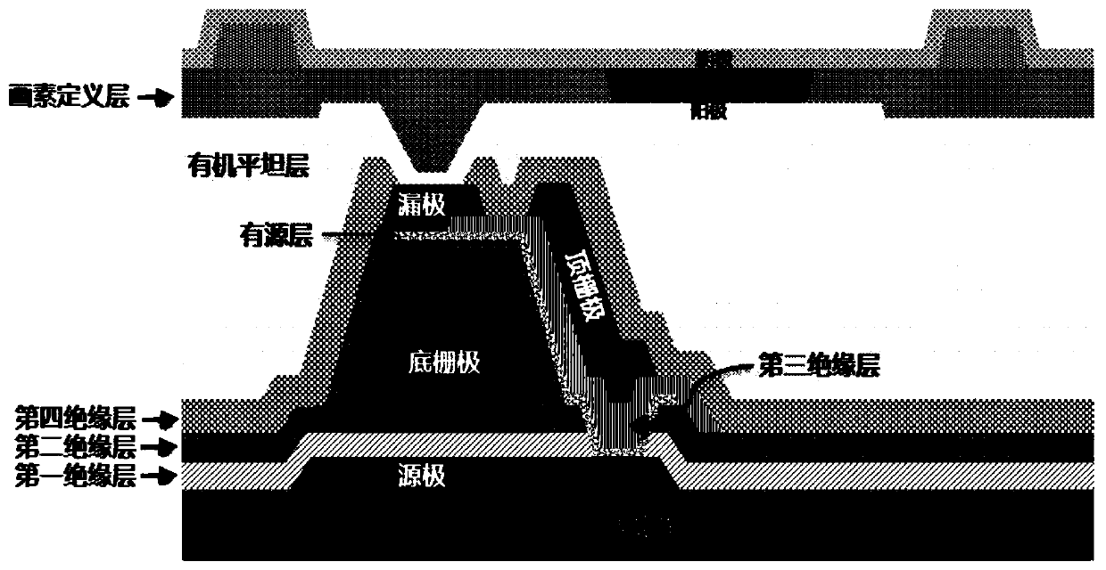
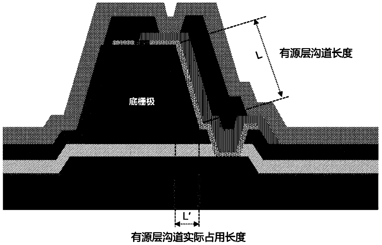
[0024] figure 1 A schematic diagram of the structure of a thin film transistor and an OLED panel thereon according to the present invention is shown, which involves a thin film transistor with a vertical structure, and the vertical structure refers to a transistor structure in which an active layer channel is formed on the side of the gate, In some existing technical solutions, the vertical structure is simplified to a "冂"-shaped structure outside the gate, which is also the origin of the name of the vertical structure. figure 2 Introduced the benefits of the vertical structure, we can see that the active layer can actually be in a range of 30°-90° oblique angle, really designed to be completely vertical is not conducive to the stabi...


PUM


Abstract

The invention discloses a thin film transistor and a manufacturing method thereof. The thin film transistor comprises a substrate and a bottom gate arranged on the substrate, an active layer is also arranged above the bottom gate, the active layer comprises a part arranged in parallel with one side surface of the bottom gate, and a top gate is also arranged on the other side of the part, oppositeto the side surface of the bottom gate, of the active layer. Different from the prior art, compared with a planar thin film transistor, the thin film transistor has the advantages that the critical dimension (CD) of the channel process of the thin film transistor can be shortened, so that the occupied area of the whole device is reduced, and the PPI of a panel is improved; and the vertical structure thin film transistor with the double-gate structure has higher electron mobility and device stability.

Description

technical field [0001] The invention relates to a new design of a TFT tube, in particular to an optimized design of a thin film transistor with a vertical structure. Background technique [0002] With the development of active-matrix organic light-emitting diode displays (AMOLED) and high-performance active-matrix liquid crystal displays (AMLCD), in order to obtain high-resolution and high-frame-rate displays, TFTs usually require higher current and voltage drive capabilities. , so how to design and fabricate high-performance and small-sized thin-film transistors has become a research topic that needs to be tackled more and more. [0003] IGZO is an amorphous oxide containing indium, gallium and zinc. The carrier mobility is 20 to 30 times that of amorphous silicon. It can greatly improve the charge and discharge rate of TFT to the pixel electrode, improve the response speed of the pixel, and have a more Fast panel refresh rate can realize ultra-high resolution TFT-LCD. At...

Claims


Application Information

Patent Timeline
Patent Type & Authority Applications(China)
IPC IPC(8): H01L29/786H01L29/423H01L21/28H01L21/34H01L21/77
CPCH01L29/78693H01L29/78696H01L29/78645H01L29/78642H01L29/66969H01L21/28008H01L29/42356H10K59/1201
Inventor 陈宇怀
Owner FUJIAN HUAJIACAI CO LTD
Why Eureka
Try Eureka