Transverse SiGe heterojunction bipolar transistor with adjustable doping concentration

A technology of heterojunction bipolar and doping concentration, which is applied in the direction of semiconductor devices, electrical components, circuits, etc., can solve the problems of sensitivity to the doping concentration level of the emitter region of the device, the influence of semiconductor process deviation, and the change of doping concentration. Achieve the effects of expanding the microwave power working range, increasing the current gain, and increasing the breakdown voltage

Active Publication Date: 2019-12-10
BEIJING UNIV OF TECH
View PDF4 Cites 2 Cited by
  • Summary
  • Abstract
  • Description
  • Claims
  • Application Information

AI Technical Summary

Problems solved by technology

At this point, the doping concentration levels of the emitter, base, and collector regions of the device become very sensitive and are highly susceptible to semiconductor process variations
Small process deviations will cause large changes in the doping concentration of the emitter, base and collector regions of the device, thereby reducing the current gain, characteristic frequency and breakdown voltage of the device, thereby degrading the electrical performance of the device

Method used


Image

  • Transverse SiGe heterojunction bipolar transistor with adjustable doping concentration
  • Transverse SiGe heterojunction bipolar transistor with adjustable doping concentration
  • Transverse SiGe heterojunction bipolar transistor with adjustable doping concentration

Examples


Embodiment

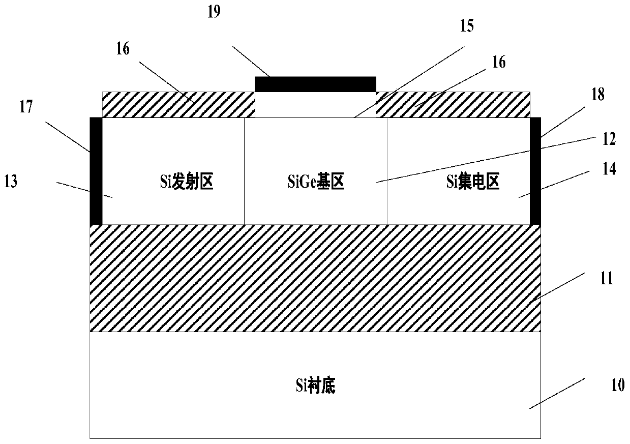
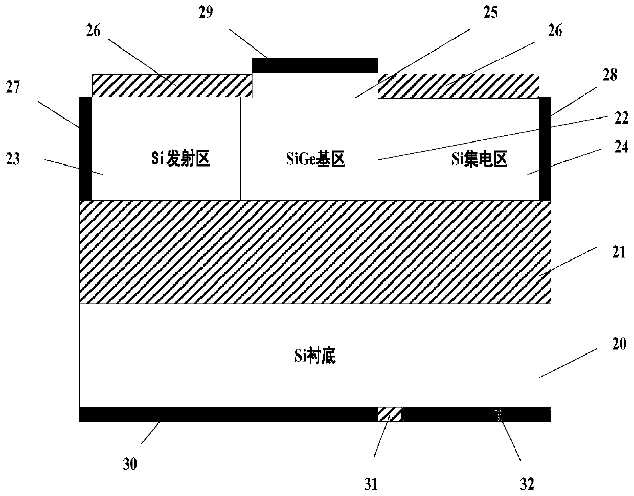
[0024] A lateral SiGe heterojunction bipolar transistor with adjustable doping concentration disclosed in the embodiment of the present invention, taking NPN type lateral SiGe HBT as an example, figure 2 Illustrates a schematic longitudinal section of an embodiment of the present invention, including a Si substrate (20) with a thickness of 20 nm and a doping concentration of 1×10 17 cm -3 ; SiO 2 The buried oxide layer (21) has a thickness of 20nm; the SiGe base region (22) has a thickness of 20nm, a width of 30nm, and a doping concentration of 1×10 19 cm -3 ; Si emitter region (23) and Si collector region (24), thickness is 20nm, and width is 30nm, and doping concentration is 2 * 10 20 cm -3 ; Wherein said SiGe base region (22), Si emitter region (23) and Si collector region (24) are positioned at SiO 2 The top of the buried oxide layer (11); the polysilicon layer (25) is located directly above the SiGe base region (22), and both sides are connected to the SiO 2 Layer ...


PUM


Abstract

The invention discloses a transverse SiGe heterojunction bipolar transistor with adjustable doping concentration. The transverse SiGe heterojunction bipolar transistor is an NPN type or PNP type transverse SiGe HBT (Heterojunction Bipolar Transistor). By applying a positive voltage to a substrate electrode below an emitter region and a base region of an NPN type device (or applying a negative voltage to a substrate electrode below an emitter region and a base region of a PNP type device), the doping concentration of the emitter region can be increased, the doping concentration of the base region can be reduced, and meanwhile, the current gain and the characteristic frequency can be improved. By applying a negative voltage to a substrate electrode below a collector region of the NPN type device (or applying a positive voltage to a substrate electrode below a collector region of the PNP type device), the doping concentration of the collector region can be reduced, and the breakdown voltage can be improved. Compared with a conventional transverse SiGe HBT, the doping concentrations of the three regions can be independently adjusted by changing the external voltages applied to the substrate electrodes below the emitter region, the base region and the collector region, so that the characteristic frequency, the current gain and the breakdown voltage are synchronously improved.

Description

technical field [0001] The invention relates to a lateral SiGe heterojunction bipolar transistor, in particular to a lateral SiGe heterojunction bipolar transistor with adjustable doping concentration used in the fields of high-speed memory, high-speed emitter-coupled logic circuit, high-speed current type logic circuit and the like. Background technique [0002] The lateral SiGe heterojunction bipolar transistor (HBT) using silicon-on-insulator (SOI) technology not only has the advantages of small substrate parasitic capacitance, low leakage current, and good high-frequency characteristics, but is also compatible with the existing SOI CMOS process , has now played an increasingly important role in the field of microwave power. [0003] figure 1 shows a schematic longitudinal cross-section of a conventional lateral SiGe HBT using SOI technology, mainly composed of Si substrate (10), SiO 2 It is composed of buried oxide layer (11), SiGe base region (12), Si emitter region (...

Claims


Application Information

Patent Timeline
Patent Type & Authority Applications(China)
IPC IPC(8): H01L29/737H01L29/36H01L29/40
CPCH01L29/737H01L29/40H01L29/36
Inventor 金冬月吴玲张万荣那伟聪孙晟杨绍萌
Owner BEIJING UNIV OF TECH
Why Eureka
Try Eureka