Dual-mode metasurface based on SOI material and dual-mode display application of dual-mode metasurface
A metasurface and top surface technology, applied in the field of micro-nano optics, can solve the problems of limited geometric structure, difficult to put into mass production and application, etc., and achieve the effect of high efficiency and maximized energy utilization
- Summary
- Abstract
- Description
- Claims
- Application Information
AI Technical Summary
Problems solved by technology
Method used
Image
Examples
Embodiment
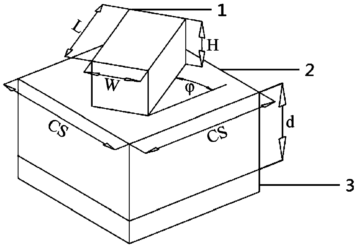
[0075] See figure 1 The nano-brick unit structure shown includes three layers, which are silicon substrate 1, fused silica medium layer 2 and nano-brick 3 constructed of crystalline silicon in sequence from bottom to top. The nano-brick array is composed of a periodic arrangement of nano-brick unit structures, and the nano-brick is in the shape of a cuboid, and its length, width and height are all sub-wavelength dimensions.
[0076] The nano-brick array structure based on SOI material can be fabricated by a conventional photolithography process in this field, and a specific preparation process will be provided below, including steps:
[0077] (1) SOI surface coated with photoresist;
[0078] (2) Using electron beam direct writing or photolithography machine to expose photoresist;
[0079] (3) After developing and etching in sequence, the array of dielectric nano-bricks is obtained on the SOI substrate (1, 2).
[0080] For the convenience of understanding, the working princi...
PUM
 Abstract
Description
Claims
Application Information


