A high-temperature-resistant broadband wave-absorbing material with dielectric gradient gradual change and its preparation method
A wave-absorbing material and high-temperature-resistant technology, applied in chemical instruments and methods, other chemical processes, etc., can solve the problems of high temperature resistance and narrow absorption frequency band, and achieve the effect of improving high temperature resistance performance and increasing absorption bandwidth.
- Summary
- Abstract
- Description
- Claims
- Application Information
AI Technical Summary
Problems solved by technology
Method used
Image
Examples
preparation example Construction
[0028] In the first aspect, the present invention provides a method for preparing a high-temperature-resistant broadband microwave-absorbing material with a gradual change in dielectric gradient. The method includes the following steps:
[0029] (1) Mix silicon carbide with high temperature resistant resin to prepare a variety of silicon carbide dispersions with different mass percentages of silicon carbide; in the present invention, the high temperature resistant resin can be, for example, phenolic resin, polyimide Resin or high temperature resistant epoxy resin;
[0030] (2) Scrape-coat the various silicon carbide dispersions obtained in step (1) on the surface of quartz fiber cloth respectively and immerse the silicon carbide dispersion into the quartz fiber cloth to obtain silicon carbide with different mass percentages. A plurality of modified quartz fiber cloths; in the present invention, a plurality of silicon carbide dispersions with different silicon carbide mass perc...
Embodiment 1
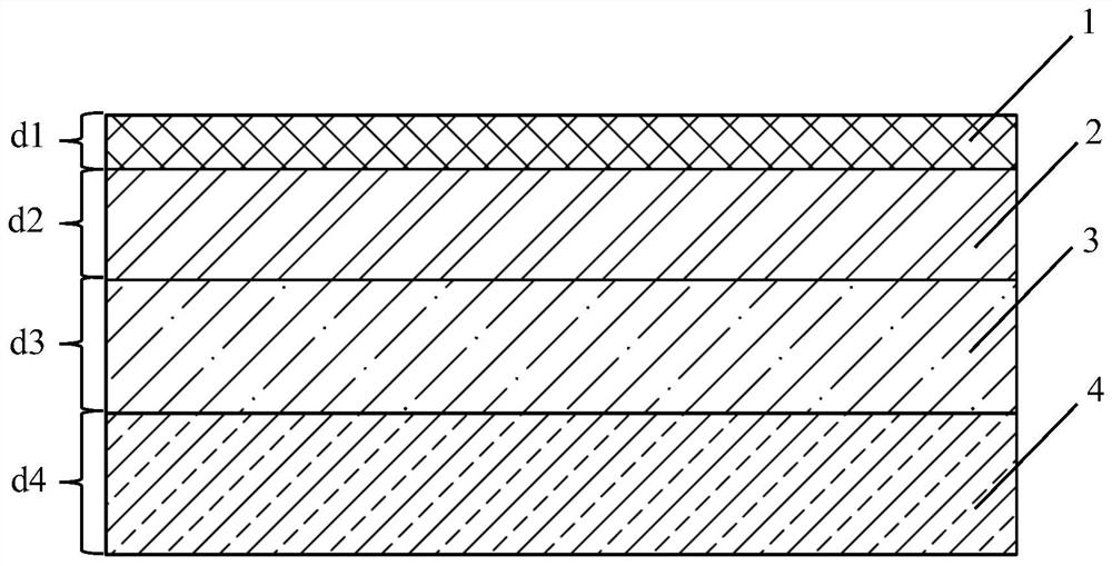
[0060] A high-temperature-resistant broadband absorbing material with a gradual change in dielectric gradient is prepared. The high-temperature-resistant broadband absorbing material has a four-layer structure, such as figure 1 As shown; the first layer is a micro-ceramic layer with a thickness of d1=1mm; the second layer is a low-concentration silicon carbide / quartz fiber composite layer with a thickness of d2=2mm; the third layer is a medium-concentration silicon carbide / quartz fiber composite layer, Thickness d3=2mm, the fourth layer is a high-concentration silicon carbide / quartz fiber composite layer, thickness d4=2mm.
[0061] The preparation process of the high-temperature-resistant broadband wave-absorbing material is as follows:
[0062] S1, silicon carbide and resin composite
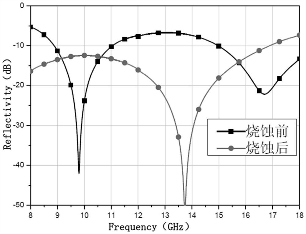
[0063] Weigh 60g of silicon carbide with a particle size of 30nm, slowly add silicon carbide to 40g of phenolic resin to form a silicon carbide dispersion with a concentration of 60%; weigh 70...
Embodiment 2
[0072] A high-temperature-resistant broadband absorbing material with a gradual change in dielectric gradient is prepared. The high-temperature-resistant broadband absorbing material has a four-layer structure, such as figure 1 As shown; the first layer is a micro-ceramic layer with a thickness of d1=1mm; the second layer is a low-concentration silicon carbide / quartz fiber composite layer with a thickness of d2=2mm; the third layer is a medium-concentration silicon carbide / quartz fiber composite layer, Thickness d3=2mm, the fourth layer is a high-concentration silicon carbide / quartz fiber composite layer, thickness d4=2mm.
[0073] The preparation process of the high-temperature-resistant broadband wave-absorbing material is as follows:
[0074] S1, silicon carbide and resin composite
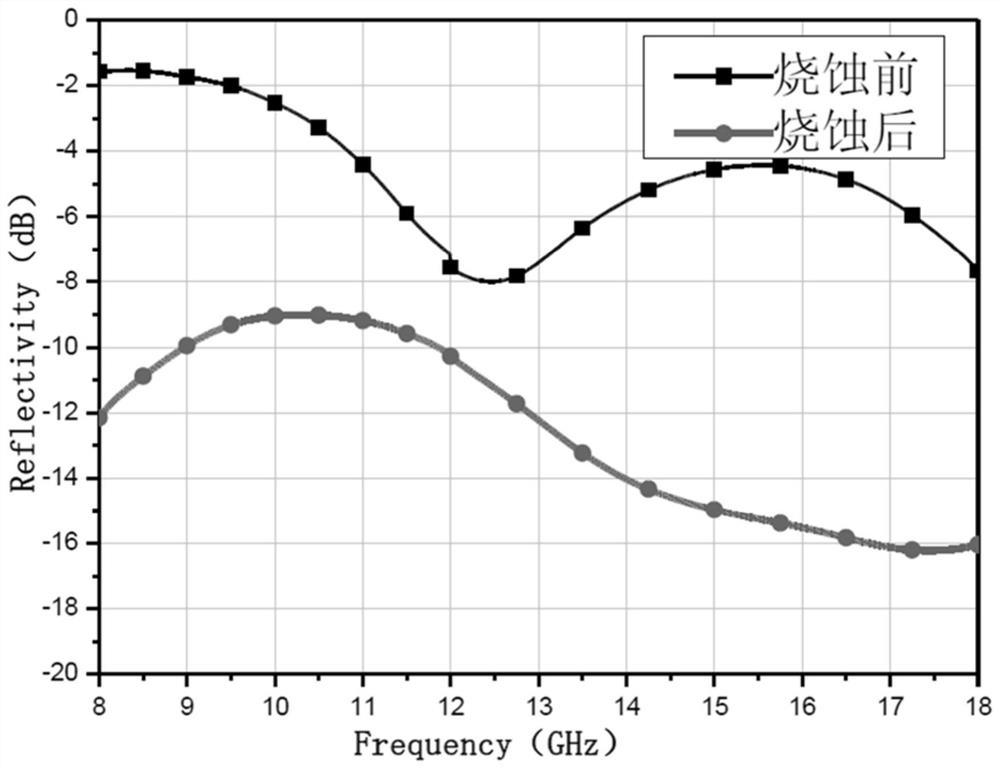
[0075] Weigh 50g of silicon carbide with a particle size of 30nm, slowly add silicon carbide to 50g of phenolic resin to form a silicon carbide dispersion with a concentration of 50%; weigh 60...
PUM
| Property | Measurement | Unit |
|---|---|---|
| particle diameter | aaaaa | aaaaa |
| thickness | aaaaa | aaaaa |
| thickness | aaaaa | aaaaa |
Abstract
Description
Claims
Application Information


