Temperature-sensitive-type terahertz detector based on phase change material and preparation method
A technology of terahertz detectors and phase change materials, which is applied in the field of terahertz photodetectors to achieve high sensitivity response, simple manufacturing process, and increase the effect of sensing ambient temperature
- Summary
- Abstract
- Description
- Claims
- Application Information
AI Technical Summary
Problems solved by technology
Method used
Image
Examples
Embodiment 1
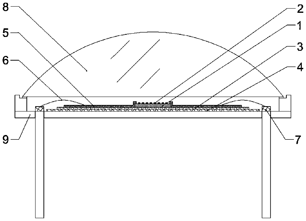
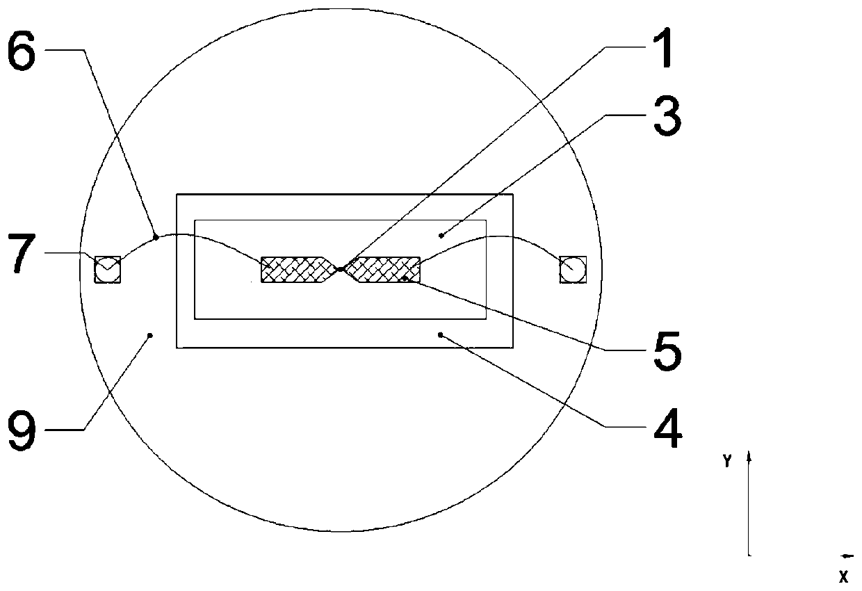
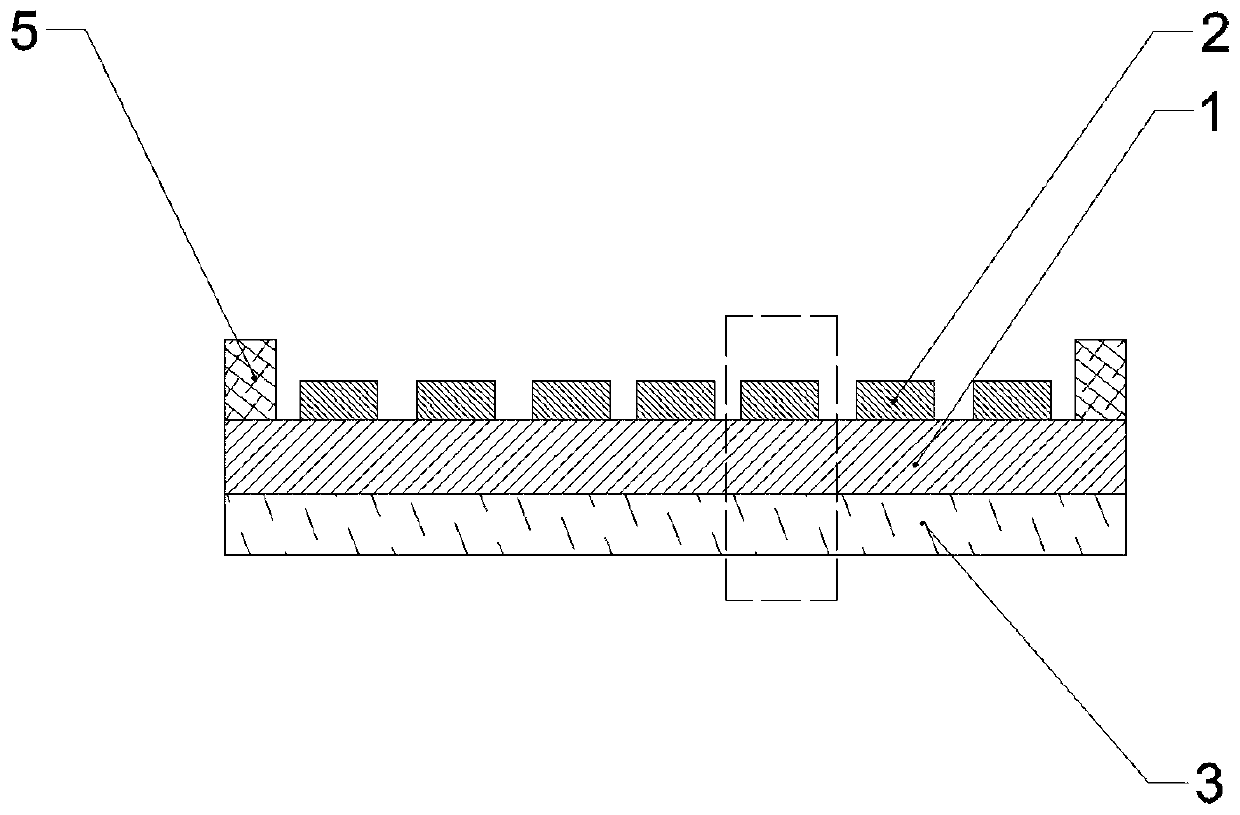
[0032]1. Select (111) crystal direction undoped single throw indium antimonide single crystal material, use epoxy resin glue to paste the single throw surface of the indium antimonide material sample on the amorphous alumina substrate 3, mechanically thin, The thickness of the indium antimonide single crystal is reduced to 10 microns. The photoresist AZ 4330 is selected, and the photolithography pattern is obtained after the photolithography process such as uniform layer exposure, development, and post-baking. Wet etching is carried out first, and an etching solution is prepared according to the ratio of HF: HAC: H2O2 = 1:1:1 to obtain an indium antimonide mesa with an etching depth of about 8um. Dry etching is then performed to remove the remaining 2um indium antimonide material layer. So far, an indium antimonide sensitive cell 1 mesa with a thickness of 10 um and a size of 90 um×20 um (length×width) has been obtained. Clean the sample sheet again with acetone, alcohol, an...
Embodiment 2
[0038] 1. Select (111) crystal direction undoped single throw indium antimonide single crystal material, use epoxy resin glue to paste the single throw surface of the indium antimonide material sample on the amorphous alumina substrate 3, mechanically thin, The thickness of the indium antimonide single crystal is reduced to 10 microns. The photoresist AZ 4330 is selected, and the photolithography pattern is obtained after the photolithography process such as uniform layer exposure, development, and post-baking. Wet etching is carried out first, and an etching solution is prepared according to the ratio of HF: HAC: H2O2 = 1:1:1 to obtain an indium antimonide mesa with an etching depth of about 8um. Dry etching is then performed to remove the remaining 2um indium antimonide material layer. So far, the indium antimonide sensitive element 1 mesa with a thickness of 10 um and a size of 120 um×20 um (length×width) has been obtained. Clean the sample sheet again with acetone, alcoh...
Embodiment 3
[0044] 1. Select (111) crystal direction undoped single throw indium antimonide single crystal material, use epoxy resin glue to paste the single throw surface of the indium antimonide material sample on the amorphous alumina substrate 3, mechanically thin, The thickness of the indium antimonide single crystal is reduced to 10 microns. The photoresist AZ 4330 is selected, and the photolithography pattern is obtained after the photolithography process such as uniform layer exposure, development, and post-baking. Wet etching is carried out first, and an etching solution is prepared according to the ratio of HF: HAC: H2O2 = 1:1:1 to obtain an indium antimonide mesa with an etching depth of about 8um. Dry etching is then performed to remove the remaining 2um indium antimonide material layer. So far, an indium antimonide sensitive cell 1 mesa with a thickness of 10 um and a size of 140 um×20 um (length×width) has been obtained. Clean the sample sheet again with acetone, alcohol, ...
PUM
| Property | Measurement | Unit |
|---|---|---|
| thickness | aaaaa | aaaaa |
| phase transition temperature | aaaaa | aaaaa |
Abstract
Description
Claims
Application Information


