Single crystal film with silicon nitride layer and preparation method thereof

A technology of silicon nitride layer and single crystal thin film, which is applied in the direction of light guide, optics, instrument, etc., can solve the problems of high loss and poor film performance, and achieve the effect of low loss, small thickness deviation and controllable thickness

Active Publication Date: 2019-12-27
JINAN JINGZHENG ELECTRONICS
View PDF5 Cites 7 Cited by
  • Summary
  • Abstract
  • Description
  • Claims
  • Application Information

AI Technical Summary

Problems solved by technology

[0004] However, since the formed plasma contains H elements, there are H elements in the deposited film, which makes many pores in the film, resulting in loose film structure, so the film performance is not good and the loss is high; while LPCVD deposits the silicon nitride functional layer The formed structure is dense and does not contain H elements. However, since the lithium niobate film cannot withstand high temperatures of 700 ° C, and the temperature of LPCVD deposition of silicon nitride is at least 700 ° C, it is impossible to directly use LPCVD to deposit a silicon nitride layer on the lithium niobate film.

Method used


Image

  • Single crystal film with silicon nitride layer and preparation method thereof
  • Single crystal film with silicon nitride layer and preparation method thereof
  • Single crystal film with silicon nitride layer and preparation method thereof

Examples


preparation example Construction

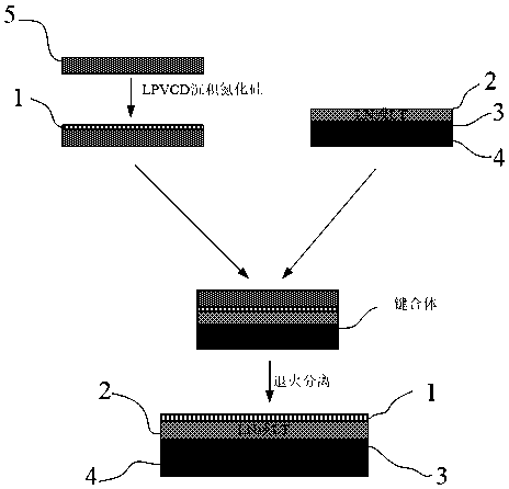
[0034] The application also includes a method for preparing a single crystal thin film with a silicon nitride layer, the flow process is as follows image 3 shown, including the following steps:

[0035] ① Deposit a layer of silicon nitride on the sacrificial silicon substrate by LPCVD to obtain the first thin film;

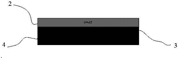
[0036] ②Prepare the second film (such as figure 2 Shown); wherein the lithium niobate / lithium tantalate thin film surface has been polished;

[0037] ③ bonding the silicon nitride layer of the first film and the lithium niobate / lithium tantalate film layer of the second film to obtain a bonded body;

[0038] ④ Grinding step ③ The sacrificial silicon substrate in the obtained bonding body is 10-20 μm, and the sacrificial silicon substrate is removed by a wet etching process to obtain a single crystal film with a silicon nitride layer.

[0039] In the preferred preparation method, in step ③, the way of bonding the silicon nitride layer of the first film and the...

Embodiment 1

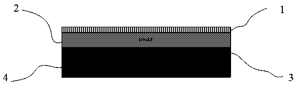
[0049] A single crystal thin film with a silicon nitride layer, including a silicon nitride layer, a lithium niobate thin film layer, a silicon oxide layer and a silicon substrate layer from top to bottom; wherein the thickness of the silicon nitride layer is 50nm, and the lithium niobate thin film The thickness of the layer is 100nm, the thickness of the silicon oxide layer is 50nm, and the thickness of the silicon substrate layer is 0.2mm; the thickness deviation of the silicon nitride layer is ≤3%, the roughness Ra<0.2nm, and the uniformity TTV<50nm.

Embodiment 2

[0051] A single crystal thin film with a silicon nitride layer, including a silicon nitride layer, a lithium tantalate thin film layer, a silicon oxide layer and a silicon substrate layer from top to bottom; wherein the thickness of the silicon nitride layer is 2 μm, and the lithium niobate thin film The thickness of the layer is 1 μm, the thickness of the silicon oxide layer is 5 μm, and the thickness of the silicon substrate layer is 1 mm; the thickness deviation of the silicon nitride layer is ≤3%, the roughness Ra<0.2nm, and the uniformity TTV<50nm.


PUM

PropertyMeasurementUnit
thicknessaaaaaaaaaa
thicknessaaaaaaaaaa
thicknessaaaaaaaaaa

Abstract

The present invention discloses a single crystal film with a silicon nitride layer and a preparation method thereof. The single crystal film with the silicon nitride layer comprises a silicon nitridelayer, a lithium niobate film layer, a silicon oxide layer and a silicon substrate layer from top to bottom. The single crystal film with the silicon nitride layer of the invention has better compatibility with the lithium niobate film, high mode limitation, low propagation loss and high power processing capacity as an optical waveguide transmission layer since silicon nitride has a good insulation effect and a wide optical transmission window. With the preparation method of the single crystal film with the silicon nitride layer in the invention, the silicon nitride waveguide is prepared by LPVCD deposition and integrated with a lithium niobate modulator, and a waveguide device with high integration level, wide bandwidth and low loss can be obtained. The preparation method of the inventionis suitable for industrial production and has a high yield.

Description

technical field [0001] The invention relates to the technical field of lithium niobate / lithium tantalate single crystal thin film, in particular to a single crystal thin film with a silicon nitride layer and a preparation method thereof. Background technique [0002] In the Internet field in recent years, optical interconnection technology has the advantages of low transmission loss, broadband, and high-speed transmission, and microring resonators, as a key technology that can realize optical interconnection, have become the key to solving problems. Due to its excellent optical properties, lithium niobate / lithium tantalate single crystal thin film can be used as a basic material for the production of high-frequency, high-bandwidth, high-integration, large-capacity, low-power optoelectronic devices and integrated optical circuits. Depositing a layer of low-loss silicon nitride on the lithium niobate / lithium tantalate film to obtain a multilayer composite film structure has br...

Claims


Application Information

Patent Timeline
Patent Type & Authority Applications(China)
IPC IPC(8): G02B6/122G02B6/13G02B6/132
CPCG02B6/122G02B6/13G02B6/132G02B2006/1204G02B2006/12045
Inventor 张涛胡文张秀全罗具廷
Owner JINAN JINGZHENG ELECTRONICS
Why Eureka
Try Eureka