Electrode substrate for transparent light-emitting device display, and manufacturing method therefor

A technology for light-emitting devices and displays, applied in semiconductor/solid-state device manufacturing, transparent dielectrics, equipment for manufacturing conductive/semiconductive layers, etc., can solve problems such as high production costs, large-scale acquisition of indium, restrictions, etc., and achieve reduction The effect of raw material costs

Active Publication Date: 2019-12-31
LG CHEM LTD
View PDF9 Cites 1 Cited by
  • Summary
  • Abstract
  • Description
  • Claims
  • Application Information

AI Technical Summary

Problems solved by technology

However, the reserves of indium, which is the main raw material of the material of the ITO transparent electrode, cannot be obtained in large quantities globally, and indium is only produced in some countries (such as China), and the production cost of indium is high
In addition, the disadvantage of indium is that the resistance value is not applied constantly, so that the expressed beam of the LED is not uniform
Therefore, transparent LEDs utilizing ITO have limitations in being used as transparent electrode materials with high performance and low cost.

Method used


Image

  • Electrode substrate for transparent light-emitting device display, and manufacturing method therefor
  • Electrode substrate for transparent light-emitting device display, and manufacturing method therefor
  • Electrode substrate for transparent light-emitting device display, and manufacturing method therefor

Examples


Embodiment approach

[0078] Hereinafter, exemplary embodiments described in this specification will be illustrated by way of examples. However, this is not intended to limit the scope of the exemplary embodiments by example.

[0079]

Embodiment 1

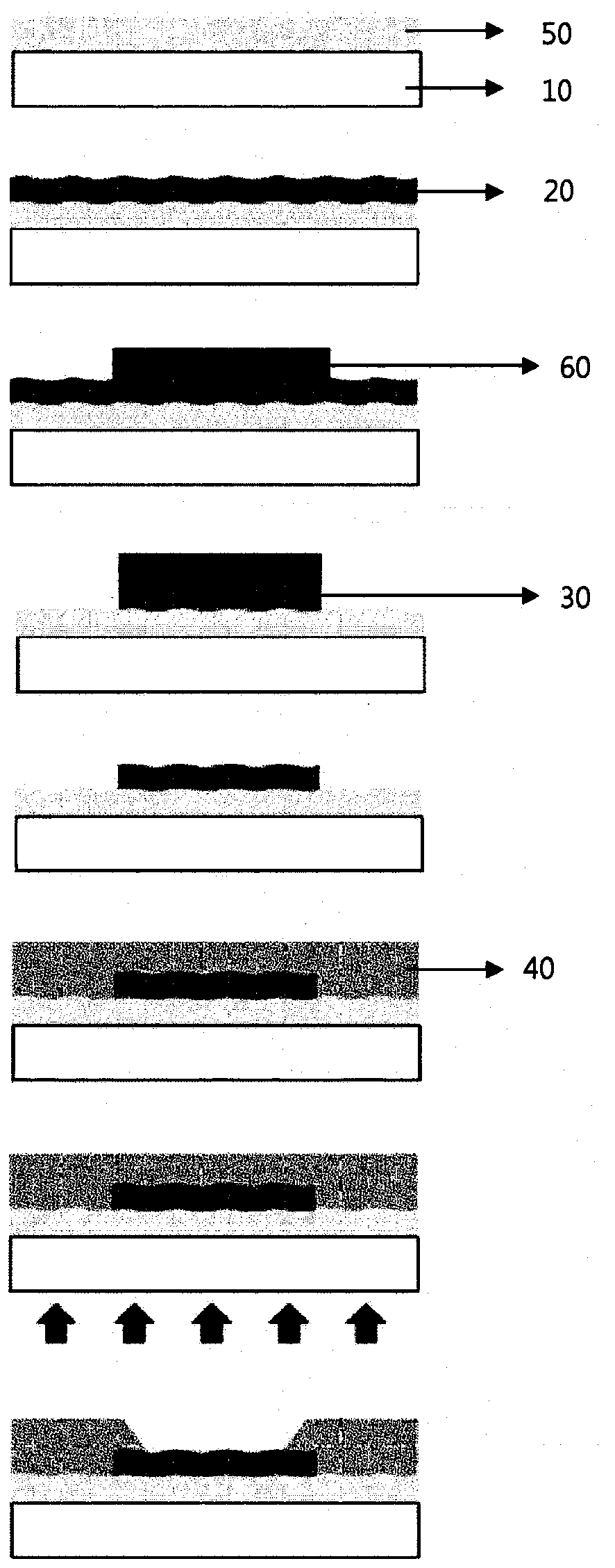
[0081] A urethane acryl-based transparent adhesive was applied on a PET film with a thickness of 250 μm by using a comma coater, followed by drying with hot air at 100° C. for 5 minutes to form an adhesive layer with a thickness of 10 μm. A PET film provided with a transparent adhesive layer and a copper foil having a thickness of 3 μm were subjected to hot roll lamination at 120° C. and 1.4 meters per minute (mpm).

[0082] A dry film resist (DFR) was laminated on the copper foil surface of the copper foil-laminated film, and then a Voronoi-style DFR pattern with a line width of 20 μm was formed through an exposure and development process.

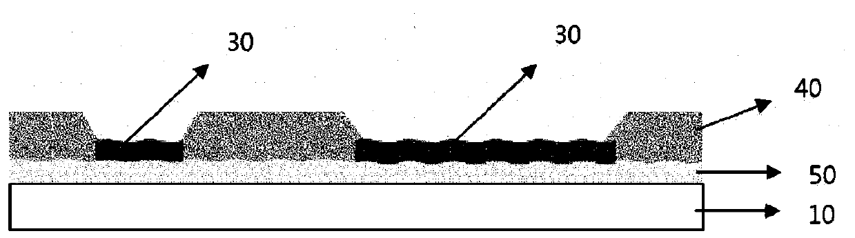
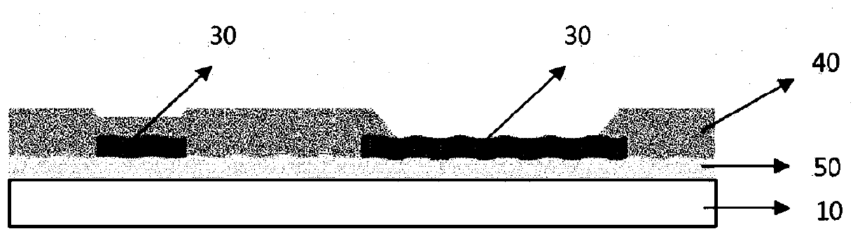
[0083] The exposed copper foil was removed by using a ferric chloride-based copper etchant, and the DFR pattern was peeled off to form a Voronoi-style copper foil pattern. In this case, the haze of the area where the copper foil pattern was not provided was 40%.

[0084] The negative transparent photosensitive resin composition was appli...


PUM

PropertyMeasurementUnit
widthaaaaaaaaaa
hazingaaaaaaaaaa
hazingaaaaaaaaaa

Abstract

A method for manufacturing an electrode substrate for a transparent light-emitting device display, according to one embodiment of the present application, comprises the steps of: laminating copper foil on a transparent substrate; etching the copper foil so as to form a copper foil pattern; forming a transparent photosensitive resin composition layer on the transparent substrate and the front surface of the copper foil pattern; and exposing at least a portion of the copper foil pattern by removing at least a portion of the transparent photosensitive resin composition layer provided on the copper foil pattern.

Description

technical field [0001] This application claims priority and benefit from Korean Patent Application No. 10-2017-0120348 filed with the Korean Intellectual Property Office on September 19, 2017, the entire contents of which are incorporated herein by reference. [0002] The present application relates to an electrode substrate for a transparent light emitting device display and a manufacturing method thereof. Background technique [0003] Recently, Korea has created a variety of exterior lighting in parks and town centers, as well as colorful signs, and provides information and attractions to city residents through the fusion of high-tech information and communication technology (ICT) and light-emitting diode (LED) technology. In particular, in a transparent LED display using an indium tin oxide (ITO) transparent electrode material, LEDs are applied between glasses or a transparent film applied with LEDs is attached to one surface of the glass, and there is an advantage that w...

Claims


Application Information

Patent Timeline
Patent Type & Authority Applications(China)
IPC IPC(8): H01B13/00H01L27/15H01L33/42H01L21/02
CPCH01L21/02H01L2933/0066H01L33/62H01L25/0753H01L33/02H05K2201/10106H05K2201/0108H05K2201/10128H05K3/0082H05K2201/09681H05K2201/0195H05K2201/2072H05K3/3452H05K2201/099H05K1/0274H01B13/0026H01L33/42H01L21/02367H01L27/156H05K3/067H05K3/287
Inventor 孙镛久李建锡李承宪
Owner LG CHEM LTD
Why Eureka
Try Eureka