Hydrogen absorption material for electronic packaging and preparation method thereof

A hydrogen-absorbing material and electronic packaging technology, applied in metal material coating process, ion implantation plating, coating, etc., can solve problems such as failure of hydrogen content exceeding the standard of sealed electronic device components, reduced solderability, increased production cycle, etc. , to achieve good hydrogen absorption capacity, high production efficiency and high reliability

Inactive Publication Date: 2020-01-17
CETC GUOJI SOUTHERN GRP CO LTD
View PDF13 Cites 2 Cited by
  • Summary
  • Abstract
  • Description
  • Claims
  • Application Information

AI Technical Summary

Problems solved by technology

Long-term high-temperature baking, on the one hand, has higher requirements on equipment, and also increases the production cycle; on the other hand, some researchers have found that after long-term high-temperature baking of the gold-plated shell, the nickel at the bottom of the coating will diffuse to the gold on the top. Oxidation occurs on the surface of the layer, resulting in reduced solderability during assembly
At the same time, components that need to be packaged, such as circulators and tantalum capacitors, cannot be dehydrogenated by high-temperature baking, and it is very easy to cause the hydrogen content of sealed electronic device components to exceed the standard and fail during use.

Method used


Image

  • Hydrogen absorption material for electronic packaging and preparation method thereof
  • Hydrogen absorption material for electronic packaging and preparation method thereof
  • Hydrogen absorption material for electronic packaging and preparation method thereof

Examples


Embodiment

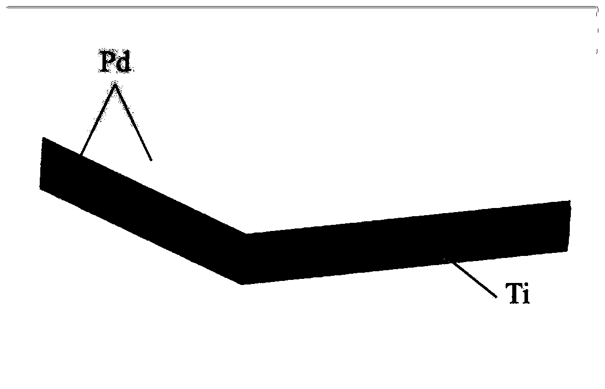
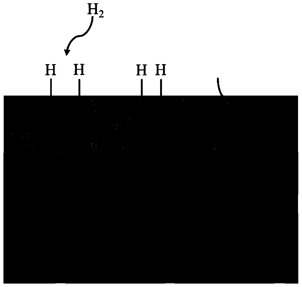
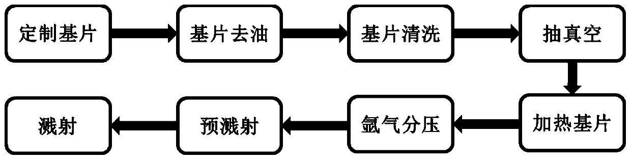
[0049] A hydrogen-absorbing material for electronic packaging, with a structure such as figure 1 shown. A titanium sheet with a purity greater than 99% is used as the sputtering substrate with a thickness of 0.2 mm. The thickness of the sputtered palladium layer is Prepare according to the above-mentioned preparation method, and the vacuum needs to be controlled at 2×10 during sputtering. -4 Below Pa.

[0050] The thickness of the Ti base material formulated by the present invention, the thickness of the Pd catalytic layer, and the sputtering process parameters are optimal parameters that comprehensively consider efficiency and effect obtained after many tests, and can ensure that the hydrogen in the atmosphere inside the sealed electronic device assembly is effectively absorbed. absorb.

[0051] The hydrogen absorbing material of the present invention is compared with common hydrogen control methods for hydrogen removal effect. The selected experimental Kovar packaging s...


PUM

PropertyMeasurementUnit
thicknessaaaaaaaaaa
purityaaaaaaaaaa

Abstract

The invention discloses a hydrogen absorption material for electronic packaging and a preparation method thereof, and mainly aims at control over the content of hydrogen in sealed electronic devices and assemblies. The hydrogen absorption material comprises a Ti substrate for playing a role of storing hydrogen and a Pd film which is combined on the Ti substrate and achieves the effects of catalytic cracking and penetration. The preparation method comprises the two steps of pretreatment of the hydrogen-storage Ti substrate and magnetron sputtering of the Pd film layer. The hydrogen absorption material can be used in various types of sealed electronic devices and assemblies, absorbs the hydrogen in the sealed devices and assemblies, and therefore, the situation that chips and the like in thesealed devices are affected by the hydrogen to lose efficacy is prevented, the production efficiency and the reliability are high, and it is not required that a packaged shell and a packaged device are additionally subjected to hydrogen removal.

Description

technical field [0001] The invention relates to a getter material for electronic packaging, in particular to a hydrogen-absorbing material for electronic packaging and a preparation method thereof. Background technique [0002] The gas composition and content in sealed electronic device components have a great impact on the performance, life and reliability of the device itself, which may easily lead to serious consequences such as reduced performance and shortened life of electronic device components. Among them, the failure caused by hydrogen is mainly manifested as: (1) accelerating the corrosion of electronic devices; (2) causing oxidation, short circuit, and burning failure of electronic components; (3) hydrogen poisoning of GaAs chips, and the functions of chips and devices are seriously degraded. Therefore, strict control of hydrogen content in sealed electronic device assemblies is very necessary. [0003] The main sources of hydrogen content in sealed electronic de...

Claims


Application Information

Patent Timeline
Patent Type & Authority Applications(China)
IPC IPC(8): C23C14/34C23C14/16C23C14/02
CPCC23C14/34C23C14/165C23C14/021C23C14/022
Inventor 董一鸣敖冬飞刘雷包雷
Owner CETC GUOJI SOUTHERN GRP CO LTD
Why Eureka
Try Eureka