LLC resonant converter and control method

A technology of a resonant converter and a control method, which is applied in the control/regulation system, the conversion of AC power input to DC power output, and the conversion of DC power input to DC power output, etc., can solve the problems of large device stress and inconvenient converter design. , to achieve the effect of small frequency conversion range, excellent comprehensive performance, and reduced loss

Inactive Publication Date: 2020-01-17
MORNSUN GUANGZHOU SCI & TECH
10 Cites 14 Cited by

AI-Extracted Technical Summary

Problems solved by technology

However, due to the presence of a boost circuit, the device stress will be g...

Method used

The present invention realizes output voltage stabilization by controlling duty cycle, realizes constant-frequency PWM control, is convenient to the design of magnetic elements such as transformer, also reduces circuit drive design difficulty and device stress, has realized the soft switch of all switching devices, Moreover, there is no leading bridge arm and lagging bridge arm, wide voltage gain range, high efficiency, and high power density. The inverter circuit can use either a full bridge or a half bridge, which can achieve a wider voltage gain range than fixed-frequency phase shifting. , to meet the needs of wide voltage gain range conversion occasions. In a wor...

Abstract

The invention discloses an LLC resonant converter and a control method, and the LLC resonant converter is lower in design difficulty, and comprises an inverter circuit, an LLC resonant cavity, a transformer and a rectification network which are sequentially connected from the input to the output. The LLC resonant cavity comprises a resonant inductor Lr, an excitation inductor Lm and a resonant capacitor Cr, and is additionally provided with a two-way switch; the resonant inductor Lr and the resonant capacitor Cr are connected in series between the first output end of the inverter circuit and the first end of the primary side coil of the transformer. The second output end of the inverter circuit is connected with the second end of the primary side coil of the transformer, the excitation inductor Lm is connected with the primary side coil of the transformer in parallel, the first end of the two-way switch is connected with the first end of the primary side coil of the transformer by being connected between the resonance inductor Lr and the resonance capacitor Cr, and the second end of the two-way switch is connected with the second end of the primary side coil of the transformer; theresonant inductor Lr is connected between the first end of the two-way switch and the first end of the primary side coil of the transformer, and the resonant capacitor Cr is connected between the first end of the two-way switch and the first output end of the inverter circuit.

Application Domain

Technology Topic

CapacitanceResonant capacitor +8

Image

  • LLC resonant converter and control method
  • LLC resonant converter and control method
  • LLC resonant converter and control method

Examples

  • Experimental program(1)

Example Embodiment

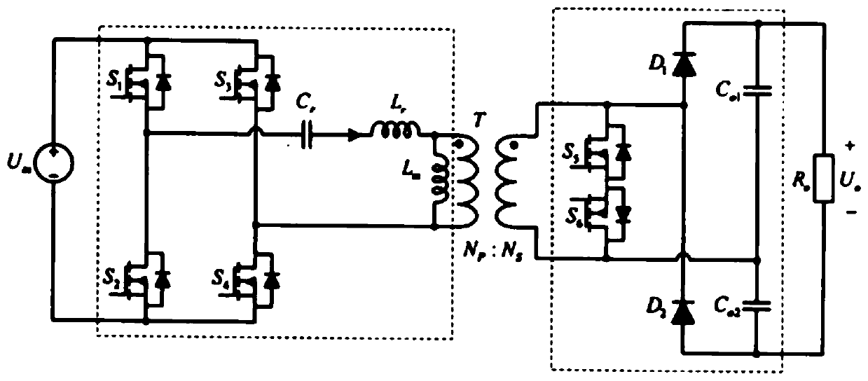
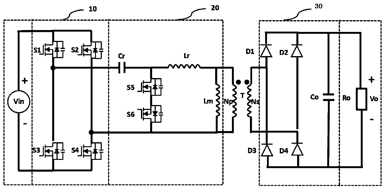
[0028] Such as image 3 As shown, the LLC resonant converter of this embodiment includes an inverter circuit 10, an LLC resonant cavity 20, a transformer T, and a rectifier network 30 that are sequentially connected from input to output. In the figure, Vin is the input power of the converter, Ro is the output load R of the converter 0.
[0029] The inverter circuit 10 is a full-bridge inverter circuit composed of a switching tube S1, a switching tube S2, a switching tube S3, and a switching tube S4. The LLC resonant cavity 20 includes a resonant inductance Lr, an excitation inductance Lm and a resonant capacitor Cr, and is additionally provided with a bidirectional switch composed of a switch tube S5 and a switch tube S6. The rectifier network 30 is a full-bridge rectifier circuit composed of 4 diodes D1-D4 in parallel to output a filter capacitor C 0 constitute.
[0030] The drain of the switch S1 is connected to the drain of the switch S2 and the positive terminal of the input power Vin, the source of the switch S1 is connected to the drain of the switch S3 and one end of the resonant capacitor Cr, and the other end of the resonant capacitor Cr is connected At one end of the resonant inductor Lr and the drain of the switch S5, the other end of the resonant inductor Lr is connected to one end of the excitation inductance Lm and one end of the primary winding Np of the transformer T, and the second end of the transformer T is connected to the other end of the excitation inductance Lm. One end, the source of the switching tube S2, the drain of the switching tube S4, the drain of the switching tube S6, the source of the switching tube S4 is connected to the source of the switching tube S3 and the negative electrode of the input power supply Vin, and the source of the switching tube S6 Connected to the source of the switching tube S5; terminal 1 of the secondary winding Ns of the transformer T is connected to the anode of the secondary rectifier diode D1 and the cathode of the secondary rectifier diode D3, and the cathode of the secondary rectifier diode D1 is connected to the secondary rectifier diode The cathode of D2, one end of the secondary side output filter capacitor Co and one end of the output load Ro, the other end of the output load Ro is connected to the other end of the secondary side output filter capacitor Co, the anode of the secondary side rectifier diode D3 and the secondary side rectifier The anode of the diode D4 and the cathode of the secondary rectifier diode D4 are connected to the anode of the secondary rectifier diode D2 and the 2 ends of the secondary winding Ns of the transformer T.
[0031] The 1 ends of the primary winding and the secondary winding of the transformer have the same name each other, and the 2 ends of the primary winding and the secondary winding of the transformer have the same name each other.
[0032] The above LLC resonant converter can adopt the following fixed-frequency PWM control method: the switching frequencies of the switching tubes S1 to S6 are equal and fixed, the switching tubes S1 and S5 are complementarily turned on, and the switching tubes S2 and S6 are complementarily turned on. S1 and the switching tube S4 are turned on and off at the same time, the switching tube S2 and the switching tube S3 are turned on and off at the same time, the duty cycle of the switching tube S1 is equal to that of the switching tube S2, and both are not greater than 0.5 and The phase difference between the two is 180°, the duty cycle of the switching tube S5 is equal to the duty cycle of the switching tube S6, both are not less than 0.5 and the phase difference between the two is 180°, the output voltage is realized by adjusting the duty cycle of the switching tube S1 The greater the duty cycle of the switch S1, the greater the output voltage gain.
[0033] In specific implementation, a reasonable dead time must be set between the switching signals of the switching tube S1 and the switching tube S5 to realize the soft switching of the switching tube S1, the switching tube S4, and the switching tube S5; the switching of the switching tube S2 and the switching tube S6 A reasonable dead time must be set between the signals to realize the soft switching of the switching tube S2, the switching tube S3, and the switching tube S6. Coss1 to Coss6 respectively represent the output capacitances to the sixth switching tubes S1 to S6.
[0034] Combine below image 3 , Explain the working process of LLC resonant converter using fixed frequency PWM control in detail.
[0035] In this embodiment, the parameters are selected as follows: Lr=220nH, Lm=800nH, Cr=82nF, and the input voltage range is 36-75VDC. The primary and secondary turns ratio of the transformer is 2:1. Figure 4 For this kind of resonant converter using fixed frequency PWM control, the main working waveform diagram, Vgs1/4 is the driving signal of the switching tube S1 and S4, Vgs2/3 is the driving signal of the switching tube S2 and S3, and Vgs5 is the switching tube S5. Drive signal, Vgs6 is the drive signal of the switch tube S6, Vc, iLr, iLm, i 0 Respectively represent the voltage across Cr, the current through Lr, the current through Lm and the through resistance R 0 的current. From Figure 4 It can be seen that the output current I of the present invention 0 The change is gentle and the device stress is small. The LLC resonant converter has six switching modes in a half cycle, respectively, as Figure 5-10 As shown (the second half cycle of the LLC resonant converter is symmetrical with the first half cycle of the working mode. It can also be seen from the waveform diagram. Generally, the description of the LLC resonant converter only describes the half cycle).
[0036] Switch mode 1[t 0 , T 1 ]: As attached Figure 5 Shown in t 0 Before time, the switching tube S6 is turned on, the switching tube S5 is turned off, and its body diode bears the reverse voltage and the reverse end; at t0, the switching tube S1 and the switching tube S4 are turned on at zero voltage; the secondary side rectifier diode D1 and the secondary side The rectifier diode D4 is turned on, and the current flowing through the diode is proportional to the difference between the resonance current and the excitation current; the voltage across the excitation inductance Lm is output clamped to nVO (n is the transformer turns ratio); the primary resonance inductance Lr is proportional to the resonance The capacitor Cr participates in resonance, the resonance current iLr is a standard sine wave and is negative, and the excitation inductance current iLm increases linearly, but is less than the resonance current iLr;
[0037] Switch mode 2[t 1 , T 2 ]: As attached Image 6 Shown in t 1 At the moment, the resonant current iLr crosses the zero point; the secondary side rectifier diode D1 and the secondary side rectifier diode D4 continue to conduct; the voltage across the excitation inductance Lm is output clamped to nV O; The primary side resonant inductance Lr and the resonant capacitor Cr participate in resonance, the resonant current iLr is a standard sine wave and is positive, and the excitation inductance current iLm increases linearly, but is less than the resonant current iLr;
[0038] Switch mode 3[t 2 , T 3 ]: As attached Figure 7 Shown in t 2 At the moment the switching tube S1 and the switching tube S4 are turned off, the resonance current iLr is still greater than the excitation inductance current iLm, the secondary side rectifier diode D1 and the secondary side rectifier diode D4 continue to conduct; the resonance current iLr is supplied to the output capacitance of the switching tube S1 and the switching tube S4 C oss1 , C oss4 Charge, output capacitor C to switch S2 and switch S3 oss2 , C oss3 Discharge, to the output capacitor C of the switch tube S5 oss5 Discharge; when the capacitance C oss5 When the voltage at both ends drops to zero, the body diode of the switching tube S5 is turned on, which provides conditions for the switching tube S5 to realize zero voltage turn-on.
[0039] Switch mode 4[t 3 , T 4 ]: As attached Picture 8 Shown in t 3 At the moment the switching tube S5 turns on at zero voltage, the switching tube S6 and the secondary side rectifier diode D1 and the secondary side rectifier diode D4 continue to conduct; the excitation inductance Lm is still clamped by the output voltage, the excitation current iLm continues to increase linearly, and the resonance current iLr decreases linearly;
[0040] Switch mode 5[t 4 , T 5 ]: As attached Picture 9 Shown in t 4 At the moment, the resonant current iLr is equal to the excitation current iLm, and the current flowing through the secondary side rectifier diode D1 naturally crosses 0. The secondary side rectifier diode D1 and the secondary side rectifier diode D4 are turned off at zero current to avoid the diode reverse recovery problem; S5 and the switch S6 continue to conduct, the excitation current and the resonance current iLr are equal and remain unchanged;
[0041] Switch mode 6[t 5 , T 6 ]: As attached Picture 10 Shown, t 5 At the moment, the switch S6 is turned off and the switch S5 continues to conduct; the resonant current iLr is equal to the excitation current iLm, and the secondary rectifier diode is still in reverse cut-off state; the resonant current iLr is supplied to the switch S1 and the output capacitor C of the switch S4 oss1 , C oss4 Charge the output capacitor C of the switching tube S2 and the switching tube S3 oss2 , C oss3 Discharge, to the output capacitor C of the switch tube S6 oss6 Charge; when the capacitor C oss2 , C oss3 When the voltage at both ends drops to 0, the body diode of the switching tube S2 and the switching tube S3 is turned on, which provides conditions for the switching tube S2 and the switching tube S3 to realize zero voltage turn-on; at t6, the switching tube S2 and the switching tube S3 realize ZVS, The circuit enters the second half cycle.
[0042] According to the description of the working process of the above converter, each switching device of the converter can realize zero-voltage turn-on, and the rectifier devices on the secondary side can also realize zero-current turn-off. There is no diode reverse recovery problem, and all switching devices are Can realize soft switching.
[0043] The two-way switch of the present invention is located on the primary side of the transformer, and there is no need to consider the isolation drive problem, which reduces the difficulty of circuit drive design. The invention changes figure 2 The position of the resonant inductor Lr and the resonant capacitor Cr turns the original boost circuit into a buck circuit, which solves the problem of greater device stress. Therefore, overall, the LLC resonant converter with the structure of the present invention reduces the design difficulty of the LLC resonant converter.
[0044] In the LLC resonant converter with the structure of the present invention, when the bidirectional switch is turned on, the energy of the resonant current is stored in the loop composed of the transformer magnetizing inductance Lm, the resonant inductance Lr and the bidirectional switch in the circulating phase, and will not flow through the resonant capacitor Cr. The resonant capacitor Cr has parasitic resistance, which is beneficial to reduce the energy loss on the parasitic resistance of the resonant capacitor Cr. The circuit structure of the present invention can further improve the working efficiency of the circuit.
[0045] The invention realizes output voltage stabilization by controlling the duty cycle, realizing fixed-frequency PWM control, facilitating the design of magnetic components such as transformers, reducing circuit drive design difficulty and device stress, and realizing soft switching of all switching devices, and there is no Leading bridge arm and lagging bridge arm, wide voltage gain range, high efficiency, high power density, the inverter circuit can use either full bridge or half bridge, which can achieve a wider voltage gain range than fixed frequency phase shift, satisfying wide The needs of voltage gain range conversion occasions. In short, the converter of the present invention has excellent overall performance.
[0046] The description of the above embodiments is only used to help understand the inventive concept of the application, and is not used to limit the present invention. For example, the switch tubes S5 and S6 of the present invention can also be connected in reverse series with common drain (the respective control timings remain unchanged), and the rectifier network Other full-wave rectifier circuits can also be used, and the above rectifier diodes can also be replaced with switching tubes, etc. In short, for those of ordinary skill in the art, any modification or equivalent made without departing from the principle of the present invention Replacement, improvement, etc. should all be included in the protection scope of the present invention.

PUM

no PUM

Description & Claims & Application Information

We can also present the details of the Description, Claims and Application information to help users get a comprehensive understanding of the technical details of the patent, such as background art, summary of invention, brief description of drawings, description of embodiments, and other original content. On the other hand, users can also determine the specific scope of protection of the technology through the list of claims; as well as understand the changes in the life cycle of the technology with the presentation of the patent timeline. Login to view more.

Similar technology patents

Classification and recommendation of technical efficacy words

  • Reduce design difficulty
  • Reduce difficulty

Projection type planar waveguide helmet-mounted displayer

ActiveCN103885184AReduce design difficultyReduce stray lightOptical light guidesHelmet-mounted displayWaveguide
Owner:BEIJING NEDPLUSAR DISPLAY TECH CO LTD

Power supply chip and method for adjusting output voltage of same

ActiveCN101968668AReal-time modification of output voltageReduce design difficultyElectric variable regulationVoltage
Owner:江苏航天龙梦信息技术有限公司

High dynamic-range image synthesis method and device

ActiveCN102420944AReduce difficultyReduce the number of imagesTelevision system detailsColor television detailsImage alignmentImage synthesis
Owner:芯鑫融资租赁(厦门)有限责任公司

Building block type aircraft carrier

InactiveCN101259876AReduce difficultySpeed up productionAircraft carriersAirplaneTakeoff
Owner:左学禹
Why Eureka
Try Eureka