Embedded grating structure-based narrow-band near-infrared thermo-electronic photoelectric detector

A technology of photodetector and grating structure, applied in the field of photoelectric sensing, can solve the problem of low photodetector responsivity, and achieve the effects of realizing narrow-band photoelectric detection, improving light absorption efficiency, and reducing thermalization loss.

Active Publication Date: 2020-01-24
SUZHOU UNIV
View PDF5 Cites 4 Cited by
  • Summary
  • Abstract
  • Description
  • Claims
  • Application Information

AI Technical Summary

Problems solved by technology

[0004] In order to solve the problem of low photodetector responsivity in the prior art, the present invention provides a na...

Method used


Image

  • Embedded grating structure-based narrow-band near-infrared thermo-electronic photoelectric detector
  • Embedded grating structure-based narrow-band near-infrared thermo-electronic photoelectric detector
  • Embedded grating structure-based narrow-band near-infrared thermo-electronic photoelectric detector

Examples


Embodiment 1

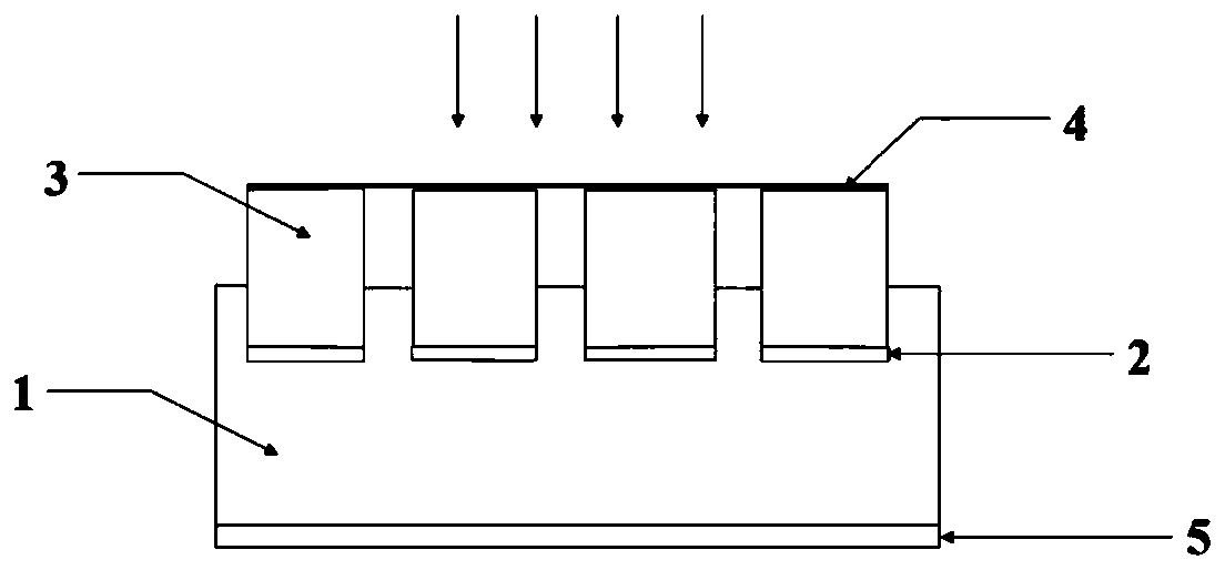
[0021] Such as figure 1 As shown, a narrow-band near-infrared thermionic photodetector based on an embedded grating structure includes a silicon substrate 1, a titanium film 2, a metal grating 3, a top conductive electrode 4, and a bottom conductive electrode 5; the titanium film and metal grating sequentially arranged on the silicon substrate; the bottom conductive electrode is connected to the silicon substrate, and the top conductive electrode is fixedly connected to the metal grating; the titanium film is used as an adhesive layer to connect the silicon substrate and the metal grating; the metal grating embedded in the silicon substrate.

[0022] Preferably, the metal grating can be one of gold, silver, copper and aluminum, and the thickness of the gold grating is 100-400 nm.

[0023] Preferably, the bottom conductive electrode can be one of indium and aluminum.

Embodiment 2

[0025] A narrow-band near-infrared thermionic photodetector based on an embedded grating structure, including a silicon substrate and a gold grating;

[0026] Specifically, there is a titanium thin film as an adhesion layer between the gold grating and the silicon substrate;

[0027] Specifically, the titanium thin film layer and the gold grating are successively arranged on the silicon substrate;

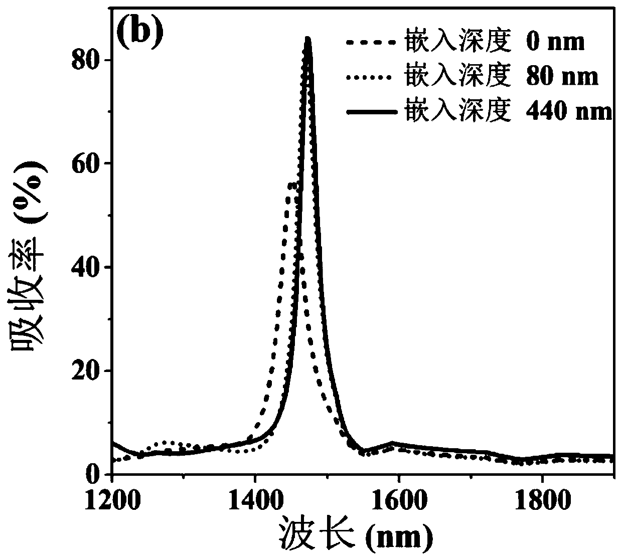
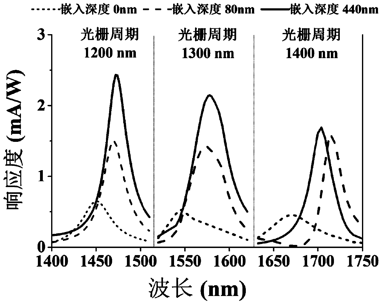
[0028] The gold grating is embedded in the silicon substrate with an embedding depth of 0-600 nm.

[0029] The gold grating is used to absorb photons and generate hot electrons. The gold grating is connected to the gold plate as the top conductive electrode, and the bottom conductive electrode is located on the back of the silicon substrate;

[0030] The embedded structure composed of gold grating and silicon substrate 1 can excite surface plasmon optical resonance, and then localize the electric field at the Schottky interface composed of gold grating and silicon substrate, which...


PUM

PropertyMeasurementUnit
Thicknessaaaaaaaaaa
Thicknessaaaaaaaaaa

Abstract

The invention belongs to the technical field of photoelectric sensing and provides an embedded grating structure-based narrow-band near-infrared thermo-electronic photoelectric detector. The inventionaims to solve the problem of the low responsivity of a photoelectric detector in the prior art. The embedded grating structure-based narrow-band near-infrared thermo-electronic photoelectric detectorcomprises a silicon substrate and a metal grating, a titanium film is arranged between the metal grating and the silicon substrate so as to serve as an adhesive layer; the metal grating is connectedto a top conductive electrode; and a bottom conductive electrode is arranged on a silicon back surface. The metal grating is embedded into the silicon substrate, so that the light absorption efficiency of metal and the generation rate of hot electrons are improved, and the thermalization loss of the hot electrons is reduced; a Schottky interface on the side surface of the grating is additionally adopted, so that the collection efficiency of the hot electrons transferred into silicon is improved, and therefore, the responsivity of the photoelectric detector is improved; and the response wavelength of the detector can be changed by adjusting the period of the metal grating, so that the wavelength-adjustable near-infrared photoelectric detector is achieved.

Description

technical field [0001] The invention relates to the technical field of photoelectric sensing, in particular to a narrow-band near-infrared thermal electron photodetector based on an embedded grating structure. Background technique [0002] In planar metals, electrons absorb the energy of incident light and transition from the ground state to a higher energy level to convert them into hot electrons, a process known as photoinduced direct excitation. However, the generation of hot electrons is extremely inefficient due to the high reflectivity of planar metals. Due to the high local electric field enhancement effect of surface plasmons, the process of generating hot electrons by exciting surface plasmons is attracting more and more attention. In metal nanostructures, electrons in the metal resonate with incident electromagnetic waves to excite surface plasmons, and hot electrons are generated in the form of electronic transitions under the energy disturbance of surface plasmo...

Claims


Application Information

Patent Timeline
IPC IPC(8): H01L31/101H01L31/0232
CPCH01L31/02327H01L31/101
Inventor 张程施嘉伟李孝峰刘添裕曹诗嘉眭博闻蔡文杰
Owner SUZHOU UNIV
Why Eureka
Try Eureka