Flexible substrate-based semiconductor epitaxial structure, VCSEL and manufacturing method
A flexible substrate and epitaxial structure technology, which is applied in the field of semiconductors, can solve the problems of semiconductor epitaxial layer growth difficulties, etc., and achieve the effects of reducing threading dislocations, easy peeling, and difficult growth
- Summary
- Abstract
- Description
- Claims
- Application Information
AI Technical Summary
Problems solved by technology
Method used
Image
Examples
Embodiment 1
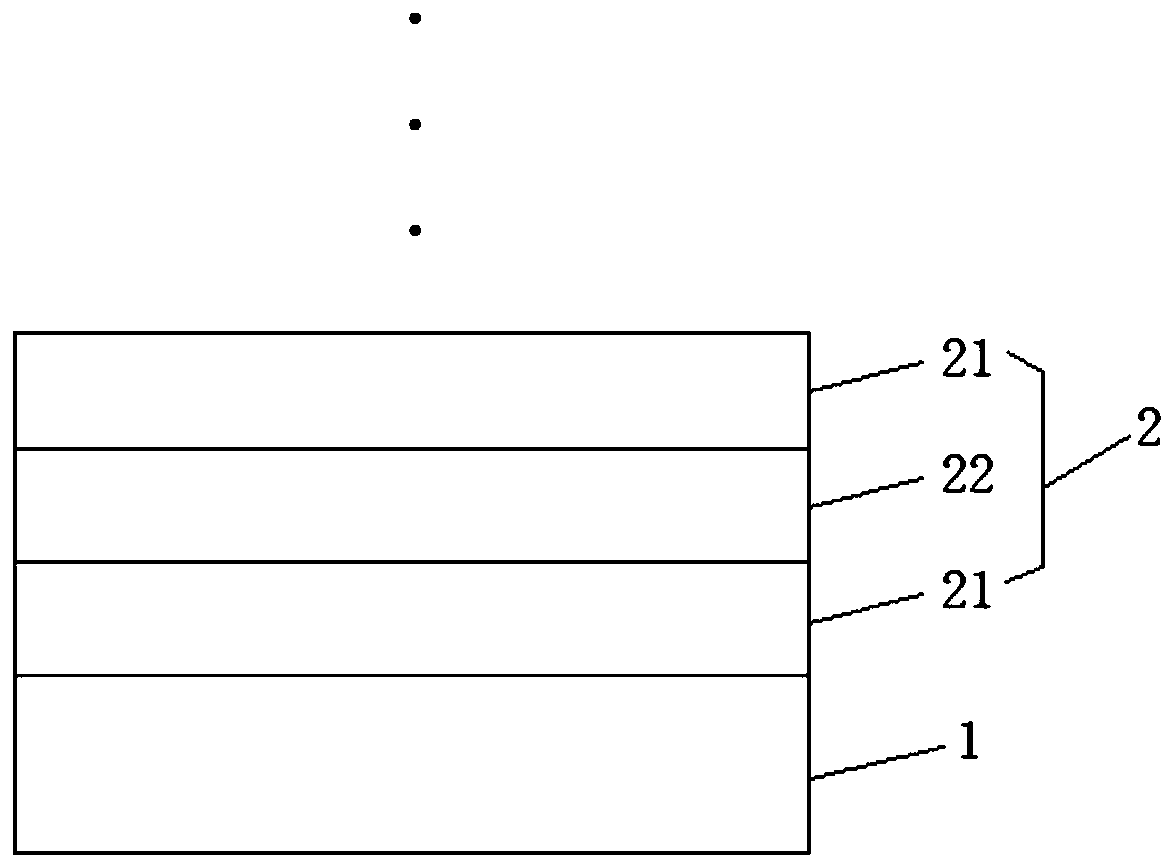
[0070] A semiconductor epitaxial structure based on a flexible substrate, such as Figure 4 Shown, comprise fluorine phlogopite substrate 1 and be located at the buffer layer 2 on fluorine phlogopite substrate 1, described buffer layer 2 comprises:
[0071] A multi-layer first GaInP buffer layer 21 and a multi-layer second GaInP buffer layer 22, the multi-layer first GaInP buffer layer 21 is sequentially arranged on the fluorophlogopite substrate 1 from bottom to top; two adjacent layers of the first GaInP buffer layer 21 and between the fluorophlogopite substrate 1 and the adjacent first GaInP buffer layer 21 are respectively provided with the second GaInP buffer layer 22 . That is, the second GaInP buffer layers 22 and the first GaInP buffer layers 21 are alternately disposed on the fluorine phlogopite substrate 1 from bottom to top.
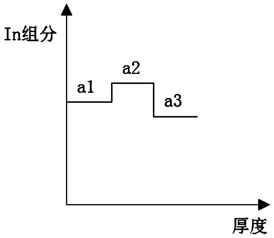
[0072] The In composition of the multilayer first GaInP buffer layer 21 decreases layer by layer from bottom to top, the In composition of t...
Embodiment 2
[0075] A method for growing a semiconductor epitaxial structure based on a flexible substrate, for making the semiconductor epitaxial structure based on the flexible substrate of the first embodiment above, comprising:
[0076] Provide a fluorine phlogopite substrate;
[0077]A buffer layer is grown on the fluorophlogopite substrate, the buffer layer includes a multi-layer first GaInP buffer layer and a multi-layer second GaInP buffer layer, and the multi-layer first GaInP buffer layer grows sequentially from bottom to top, two adjacent The second GaInP buffer layer is respectively provided between the first GaInP buffer layers and between the fluorine phlogopite substrate and the adjacent first GaInP buffer layer. Specifically, the buffer layer comprising multiple first GaInP buffer layers and multiple second GaInP buffer layers can be formed by alternately growing the second GaInP buffer layer and the first GaInP buffer layer multiple times on the fluorophlogopite substrate....
Embodiment 3
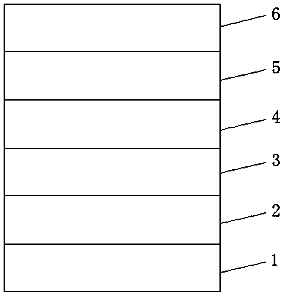
[0079] A VCSEL, comprising the semiconductor epitaxial structure based on the flexible substrate described in the first embodiment above, further comprising: an N-type DBR layer 3 sequentially stacked on the buffer layer 2 from bottom to top, a first separation limiting heterogeneous Junction 7, multi-quantum well layer 4, second separation confinement heterojunction 8, oxide layer 5 and P-type DBR layer 6, the structure diagram is as follows Figure 6 shown.
PUM
| Property | Measurement | Unit |
|---|---|---|
| Thickness | aaaaa | aaaaa |
Abstract
Description
Claims
Application Information


