Touch sensor, preparation method thereof and touch display screen

A touch sensor and touch area technology, which is applied in the field of display screens, can solve the problems of being unsuitable for large-scale promotion and application, the impact of chemical etching environment is large, and the difficulty of reducing the frame, etc., to achieve high metal film uniformity, improve Conductivity, effect of narrow linewidth

Inactive Publication Date: 2020-02-04
盈天实业(深圳)有限公司
View PDF10 Cites 0 Cited by
  • Summary
  • Abstract
  • Description
  • Claims
  • Application Information

AI Technical Summary

Problems solved by technology

At the same time, with people's pursuit of foldable screens, it is relatively more difficult to reduce the width of the frame while maintaining the basic functions and strength, so it is difficult to meet the above requirements at the same time.
[0003] At present, the industry's practice for metal thin leads is to use silk screen printing process and chemical etching, and the silver paste processed by the silk screen process is thick (about 3 μm ~ 5 μm), uneven, and prone to 10 μm ~ 20 μm granular agglomerates or foreign matter
The etched line width after silk screen printing silver paste is usually 30 μm, it is difficult to process a thinner 15 μm line on the basis of ensuring the yield rate, and chemical etching has a great impact on the environment, so it is not suitable for large-scale application

Method used


Image

  • Touch sensor, preparation method thereof and touch display screen
  • Touch sensor, preparation method thereof and touch display screen
  • Touch sensor, preparation method thereof and touch display screen

Examples


preparation example Construction

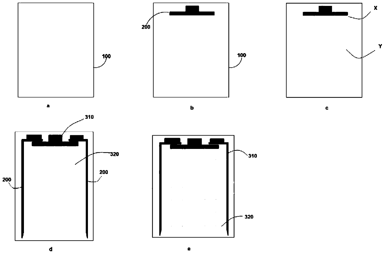
[0027] A method for preparing a touch sensor according to an embodiment of the present invention includes the following steps:

[0028] S101: Provide a substrate, the substrate is a transparent conductive flexible film with a conductive surface, and the conductive surface is silver nanowires or carbon nanotubes;

[0029] The type of substrate is not particularly limited, and a flexible transparent substrate commonly used in the art can be used. The substrate has a conductive surface and can be prepared by depositing a conductive layer on a flexible transparent substrate. For example, the substrate can be prepared by using commercially available CPI ( Colorless Polyimide, colorless polyimide), COP (Cyclo Olefin Polymer, cycloolefin polymer), etc., can deposit carbon nanotubes or nano silver wires on it to form a conductive coating.

[0030] By using silver nanowires or carbon nanotubes as the conductive surface, it is conducive to ink deposition, and then can process thinner me...

Embodiment 1-1~ Embodiment 1-4

[0069] Preparation:

[0070] (1) Provide a substrate, the substrate is a transparent conductive flexible film with two conductive surfaces, the two conductive surfaces are respectively the first conductive surface and the second conductive surface, and the film materials are as shown in Table 1;

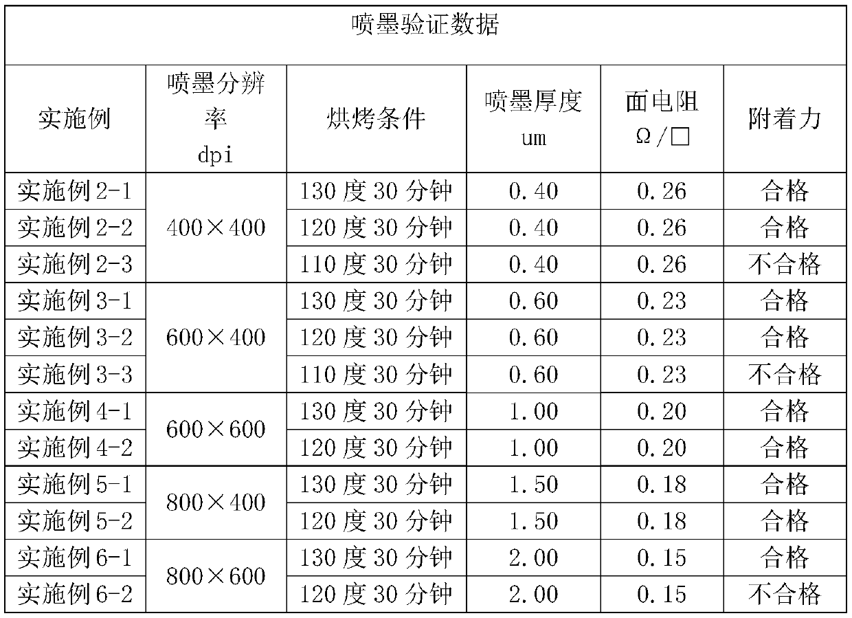
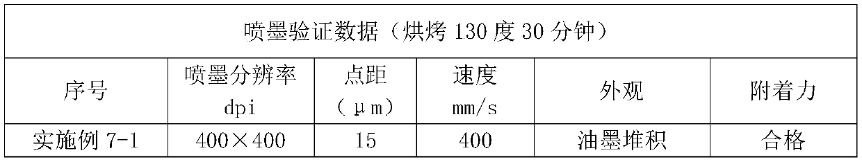
[0071] (2) Inkjet printing, containing nano-silver paste in the ink; inkjet printing ink to the specified area of ​​the first conductive surface of the film (the distance between the nozzle and the film is 20 μm, the speed is 400mm / s, and the ink thickness is 0.4 μm), cured at 130°C for 30 minutes to form a conductive metal area, and the area of ​​the substrate where no conductive metal area is formed is the touch area;

[0072] (3) Laser etching, using laser to etch the conductive metal area and the touch area to form the first graphic circuit, wherein the laser wavelength is 355nm, the laser energy is 0.25W, and the laser speed is 900mm / s;

[0073] (4) Protect the processed circui...


PUM

PropertyMeasurementUnit
thicknessaaaaaaaaaa
thicknessaaaaaaaaaa
wavelengthaaaaaaaaaa

Abstract

The invention relates to a touch sensor and a preparation method thereof, and a touch display screen, the preparation method of the touch sensor comprises the following steps: providing a substrate, the substrate being a transparent conductive flexible film with a conductive surface, and the conductive surface being a silver nanowire or a carbon nanotube; depositing ink in a designated area on theconductive surface of the substrate in an ink-jet printing mode and curing to form a conductive metal area, and the area, where the conductive metal area is not formed, of the substrate being a toucharea; and etching the conductive metal region and the touch region by adopting a laser etching mode so as to respectively form a first graphic circuit and a second graphic circuit which are connectedwith each other in the conductive metal region and the touch region. According to the preparation method of the touch sensor, the flexible foldable touch sensor with an ultra-narrow frame can be processed.

Description

technical field [0001] The invention relates to the technical field of display screens, in particular to a touch sensor, a preparation method thereof, and a touch display screen. Background technique [0002] As electronic devices pursue higher and higher screen ratios, the requirements for the thickness of the frame of the sensor (Sensor) of the touch screen are becoming more and more stringent, especially the metal leads inside the frame. At the same time, with people's pursuit of foldable screens, it is relatively more difficult to reduce the width of the frame while maintaining the basic functions and strength, so it is difficult to meet the above requirements at the same time. [0003] At present, the industry's practice for metal thin leads is to use silk screen printing process and chemical etching, and the silver paste processed by the silk screen process is thick (about 3 μm ~ 5 μm), uneven, and prone to 10 μm ~ 20 μm granular agglomerates or foreign matter. The e...

Claims


Application Information

Patent Timeline
Patent Type & Authority Applications(China)
IPC IPC(8): G06F3/041
CPCG06F3/041
Inventor 黄荣兆邝建邦温扬志汤飞堦文星凯
Owner 盈天实业(深圳)有限公司
Why Eureka
Try Eureka