Preparation method of DFB semiconductor laser capable of working in wide temperature range

A laser and semiconductor technology, applied in the field of optical communication, can solve the problems of high cost, large temperature drift coefficient, large wavelength drift deviation, ridge waveguide structure DFB, etc., to improve high temperature characteristics, realize wide temperature operation, and improve limit ability Effect

Active Publication Date: 2020-02-04
FUJIAN Z K LITECORE LTD
View PDF6 Cites 18 Cited by
  • Summary
  • Abstract
  • Description
  • Claims
  • Application Information

AI Technical Summary

Problems solved by technology

InP/AlGaInAs generally adopts a ridge structure, but because the gain curve of the AlGaInAs material has a large drift coefficient with temperature, it is difficult to prepare a laser with a wide temperature range
[0004] Generally, InP-based DFB lasers need to work in a wide temperature range without cooling single-mode to ensure the application of the laser in various environments; for ridge waveguide structure lasers, the wavelength of DFB single-mode emission is due to temperature changes. The drift...

Method used


Image

  • Preparation method of DFB semiconductor laser capable of working in wide temperature range

Examples


Embodiment Construction

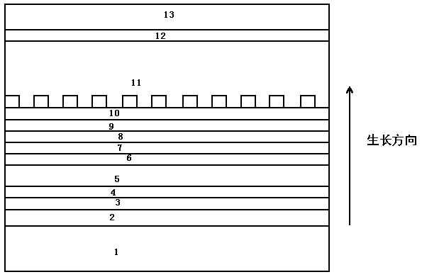
[0020] The present invention will be further described below in conjunction with the accompanying drawings and embodiments.

[0021] It should be pointed out that the following detailed description is exemplary and intended to provide further explanation to the present application. Unless defined otherwise, all technical and scientific terms used herein have the same meaning as commonly understood by one of ordinary skill in the art to which this application belongs.

[0022] It should be noted that the terminology used here is only for describing specific implementations, and is not intended to limit the exemplary implementations according to the present application. As used herein, unless the context clearly dictates otherwise, the singular is intended to include the plural, and it should also be understood that when the terms "comprising" and / or "comprising" are used in this specification, they mean There are features, steps, operations, means, components and / or combinatio...


PUM

PropertyMeasurementUnit
Thicknessaaaaaaaaaa
Thicknessaaaaaaaaaa
Thicknessaaaaaaaaaa

Abstract

The invention relates to a preparation method of a DFB semiconductor laser capable of working in a wide temperature range, which comprises the steps of sequentially growing a buffer layer, a lower waveguide structure, a lower electron barrier layer, an InGaAsP and AlGaInAs mixed quantum well, an upper electron barrier layer, an upper waveguide structure, a spacer layer, a long-wavelength grating layer and a grating protection layer on an InP substrate so as to complete the preparation of a primary epitaxial wafer; then preparing a uniform grating on the primary epitaxial wafer, and growing thegrating to form a complete epitaxial wafer; and preparing a DFB laser by adopting a conventional ridge waveguide structure process to realize the DFB semiconductor laser working in a wide temperaturerange. According to the invention, the InGaAsP and AlGaInAs mixed quantum well is adopted, the characteristics of high limiting efficiency of an AlGaInAs high-temperature carrier and small temperature drift coefficient of an InGaAsP quantum well gain spectrum are fully utilized to realize single-mode operation of the laser in a wide temperature range, and the long-wavelength grating layer with absorption characteristics is introduced at the same time to increase the absorption of the grating to the FP mode gain, thereby further inhibiting FP oscillation initiation, and realizing the single-mode laser chip capable of working in a wide temperature range.

Description

technical field [0001] The invention relates to the field of optical communication, in particular to a preparation method of a wide temperature working DFB semiconductor laser. Background technique [0002] With the rapid development of optical fiber communication, uncooled wide temperature single-mode laser will become the mainstream optical device in the field of optical communication in the future, and it is the key device for long-distance and large-capacity optical fiber communication. It is widely used in fields such as access network and data resurgence. [0003] Usually DFB lasers use InP / InGaAsP and InP / AlGaInAs material systems; due to the high temperature characteristics of InGaAsP quantum wells, InP / InGaAsP lasers usually use buried heterojunction structures, which greatly increases the cost of laser preparation. InP / AlGaInAs generally adopts a ridge structure. However, because the gain curve of AlGaInAs material has a large drift coefficient with temperature, i...

Claims


Application Information

Patent Timeline
IPC IPC(8): H01S5/12H01S5/343
CPCH01S5/12H01S5/3434H01S5/34366
Inventor 薛正群杨重英高家敏吴林福生李敬波
Owner FUJIAN Z K LITECORE LTD
Why Eureka
Try Eureka