Multiplication type organic photoelectric detector based on AIE material and preparation method thereof

A photodetector, an organic technology, applied in photovoltaic power generation, electrical solid-state devices, semiconductor/solid-state device manufacturing, etc., to achieve the effect of simple manufacturing process, high detection sensitivity, and widening applications

Active Publication Date: 2020-02-21
SOUTH CHINA UNIV OF TECH
View PDF7 Cites 1 Cited by
  • Summary
  • Abstract
  • Description
  • Claims
  • Application Information

AI Technical Summary

Problems solved by technology

However, the application of AIE materials to the field of photodetectors has not been reported so far

Method used


Image

  • Multiplication type organic photoelectric detector based on AIE material and preparation method thereof
  • Multiplication type organic photoelectric detector based on AIE material and preparation method thereof
  • Multiplication type organic photoelectric detector based on AIE material and preparation method thereof

Examples


Embodiment 1

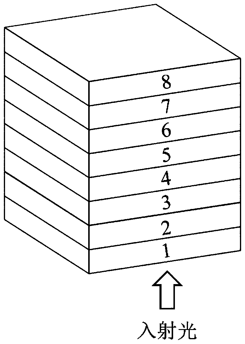
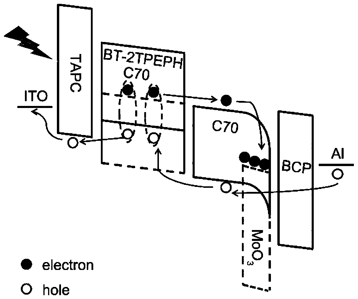
[0036] Such as figure 1 As shown, a multiplication-type organic photodetector based on aggregation-induced luminescence materials includes a transparent substrate 1, an anode 2, a hole transport layer 3, an active layer 4, a spacer layer 5, and an electron-trapping layer 6 in sequence along the direction of incident light. , electron transport layer 7, and metal cathode 8;

[0037] In this embodiment, the transparent substrate is glass; the anode is indium tin oxide (ITO); the hole transport layer is TAPC with a thickness of 40nm; the active layer is an electron donor material and an electron acceptor. The blend film of the bulk material has a thickness of 80nm. Wherein, the electron donor material is AIE1, and the electron acceptor material is C 70 , the mass concentration of the electron donor material in the active layer is 50%; the spacer layer is C 70 , whose thickness is 50nm; the electron-trapping layer is C 70 with MoO 3 The blended layer, whose thickness is 10 nm...

Embodiment 2

[0046] In this embodiment, the transparent substrate is glass; the anode is indium tin oxide (ITO); the hole transport layer is TAPC with a thickness of 40nm; the active layer is an electron donor material and an electron acceptor. The blend film of the bulk material has a thickness of 80nm. Wherein, the electron donor material is AIE2, and the electron acceptor material is C 70 , the mass concentration of the electron donor material in the active layer is 50%; the spacer layer is C 70 , whose thickness is 50nm; the electron-trapping layer is C 70 with MoO 3 The blended layer, whose thickness is 10 nm, MoO 3 The doping mass concentration is 10%; the electron transport material is BCP, and its thickness is 10nm; the cathode is metal aluminum, and its thickness is 100nm.

[0047] The specific preparation method of the multiplication type organic photodetector based on the aggregation-induced luminescence material in this embodiment is as follows:

[0048] First, lithographi...


PUM

PropertyMeasurementUnit
thicknessaaaaaaaaaa
thicknessaaaaaaaaaa
thicknessaaaaaaaaaa

Abstract

The invention belongs to the field of photoelectric devices, and discloses a multiplication type organic photoelectric detector based on an AIE material and a preparation method thereof. The organic photoelectric detector structure sequentially comprises a transparent substrate, an anode, a hole transport layer, an active layer, a spacer layer, an electron capture layer, an electron transport layer and a metal cathode; the active layer is a blending layer of an electron donor material AIE1 or AIE2 and an electron acceptor material C60 or C70; the spacing layer is C60 or C70; and the electron capture layer is a blending layer of C60 or C70 and MoO3. According to the invention, the AIE material is used as the active layer for the first time, the high-efficiency multiplication type organic photoelectric detector is prepared by using a trapped electron induced hole tunneling injection mechanism, the external quantum conversion efficiency is 60840%, the normalized detection rate is 3.08*1012 Jones, and the application of the AIE material in the field of photoelectric devices is expanded.

Description

technical field [0001] The invention belongs to the field of photoelectric devices, and in particular relates to an AIE material-based multiplication type organic photodetector and a preparation method. Background technique [0002] A photodetector is an optoelectronic device that converts an optical signal into an electrical signal. Compared with inorganic photodetectors, organic photodetectors have attracted extensive attention because of their advantages such as light weight, low cost, adjustable response spectrum range, wide range of material selection, good flexibility, and easy fabrication into large-area devices. At present, the organic photodetectors reported in the literature are mainly photodiode type, that is, the organic material absorbs solar photons to generate excitons, which diffuse to the interface of the acceptor material and dissociate into free carriers, and then carry current The electrons are collected by the electrode, thereby generating a photogenera...

Claims


Application Information

Patent Timeline
Patent Type & Authority Applications(China)
IPC IPC(8): H01L51/42H01L51/46H01L51/48
CPCH10K85/211H10K85/636H10K85/633H10K85/657H10K30/00Y02E10/549
Inventor 马东阁虢德超杨德志唐本忠徐增
Owner SOUTH CHINA UNIV OF TECH
Why Eureka
Try Eureka