Optical method for measuring resistivity of silicon wafer in non-contact manner

A non-contact, optical method technology, applied in the direction of measuring resistance/reactance/impedance, measuring electrical variables, measuring devices, etc., can solve the problem of inability to do full-coverage scanning measurement of large-size wafers and the inability to measure wafer resistance Rate and other issues

Inactive Publication Date: 2020-03-31
UNIV OF ELECTRONIC SCI & TECH OF CHINA
View PDF4 Cites 5 Cited by
  • Summary
  • Abstract
  • Description
  • Claims
  • Application Information

AI Technical Summary

Problems solved by technology

However, the disadvantages of the four-probe method are also obvious: first, the four-probe method is a contact measurement method, and the process of contacting the probe with the sample will inevitably introduce damage and pollution; Wafers with an insulating layer (such as silicon wafers through surface oxidation passivation), the four-probe method cannot measure the volume resistivity of the wafer unless

Method used


Image

  • Optical method for measuring resistivity of silicon wafer in non-contact manner
  • Optical method for measuring resistivity of silicon wafer in non-contact manner
  • Optical method for measuring resistivity of silicon wafer in non-contact manner

Examples


Embodiment Construction

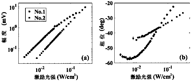
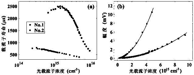
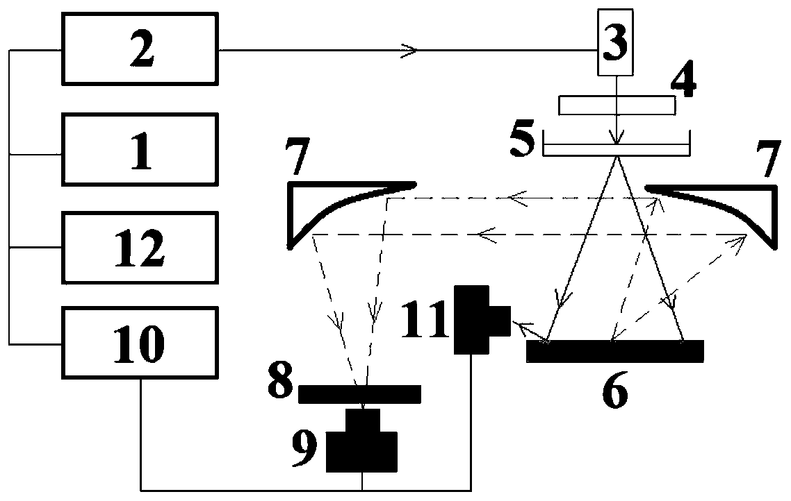
[0021] Combine below Figure 1-3 A non-contact optical method for measuring the resistivity of a silicon wafer proposed by the present invention is specifically described. However, it should be understood that the accompanying drawings are only provided for better understanding of the present invention, and should not be construed as limiting the present invention. The specific implementation steps are as follows:

[0022] (1) Build the experimental system. build as figure 1 The optical experimental system for the non-contact measurement of silicon wafer resistivity shown includes a function generator 1, an excitation laser 2, a beam collimator 3, an adjustable neutral filter 4, a uniform beam expander 5, and an off-axis parabola Mirror 7, long pass filter 8, two photodetectors 9 and 11, lock-in amplifier 10, computer 12.

[0023] a. Connect the function generator to the laser, and set the safe range of the output signal amplitude of the function generator based on the dri...


PUM


Abstract

The invention discloses an optical method for measuring resistivity of a silicon wafer in a non-contact manner, which comprises the following steps of exciting the silicon wafer by using laser which is periodically modulated in intensity and has photon energy greater than the width of a silicon forbidden band after collimation and beam expansion, and generating free electron/hole pairs with periodically changed concentration in the silicon wafer; collecting near-infrared fluorescence signals emitted by free electron/hole pairs through radiation recombination by a group of off-axis parabolic mirrors, recording by a near-infrared photoelectric detector and demodulating by a lock-in amplifier, and obtaining the amplitude and phase of the fluorescence signals; obtaining a group of intensity scanning fluorescence signals by continuously changing the average excitation light intensity, and recording the relative change of the excitation light intensity by another photoelectric detector in real time; solving the balanced majority carrier concentration of the silicon wafer by analyzing the intensity scanning data, and then obtaining the resistivity of the silicon wafer. According to the method, the resistivity of the silicon wafer can be measured in a non-contact mode, and an all-optical, lossless and quantitative characterization method is provided for wafer online monitoring/detection in the semiconductor manufacturing industry.

Description

technical field [0001] The invention relates to the field of semiconductor material characteristic detection, in particular to an optical method for non-contact, non-destructive and quantitative measurement of silicon wafer resistivity. Background technique [0002] Resistivity is one of the important parameters to characterize the conductivity of doped semiconductor materials. In today's integrated circuit industry and photovoltaic energy industry production lines, measuring the resistivity of semiconductor materials has become a routine procedure. There are many methods for measuring resistivity. Among them, the four-probe method is a standard method widely used in the global semiconductor industry. Its advantages are simple equipment, high precision, and no strict requirements on the shape of the sample. However, the disadvantages of the four-probe method are also obvious: first, the four-probe method is a contact measurement method, and the process of contacting the pro...

Claims


Application Information

Patent Timeline
IPC IPC(8): G01R27/02
CPCG01R27/02
Inventor 孙启明王静高椿明雷晓轲
Owner UNIV OF ELECTRONIC SCI & TECH OF CHINA
Why Eureka
Try Eureka