Solid dielectric for filter and its surface metallization process and dielectric filter

A solid medium, surface metal technology, applied in the field of communication, can solve the problems of reducing device performance, cracking of metal film layer, easy to be worn out, etc.

Active Publication Date: 2022-01-11
上海德门信息技术有限公司
View PDF5 Cites 0 Cited by
  • Summary
  • Abstract
  • Description
  • Claims
  • Application Information

AI Technical Summary

Problems solved by technology

However, the matching degree of thermal expansion coefficient and lattice constant between silver and microwave ceramics is not high. In order to strengthen its adhesion on the surface of solid media, it is necessary to increase the thickness appropriately, which will inevitably lead to high manufacturing costs; on the other hand , the metal silver conductor layer is directly exposed on the outer surface of the medium, which is easy to be worn and corroded, which will affect the signal transmission performance of the solid medium when it is used as a dielectric filter; There will be interface reaction, diffusion or deformation between the electrodes, which will easily cause defects such as cracking and delamination of the metal film layer, and reduce the performance of the device; therefore, there is currently no scheme to replace precious metals with multi-layer metal layers

Method used


Image

  • Solid dielectric for filter and its surface metallization process and dielectric filter
  • Solid dielectric for filter and its surface metallization process and dielectric filter
  • Solid dielectric for filter and its surface metallization process and dielectric filter

Examples


Embodiment 1

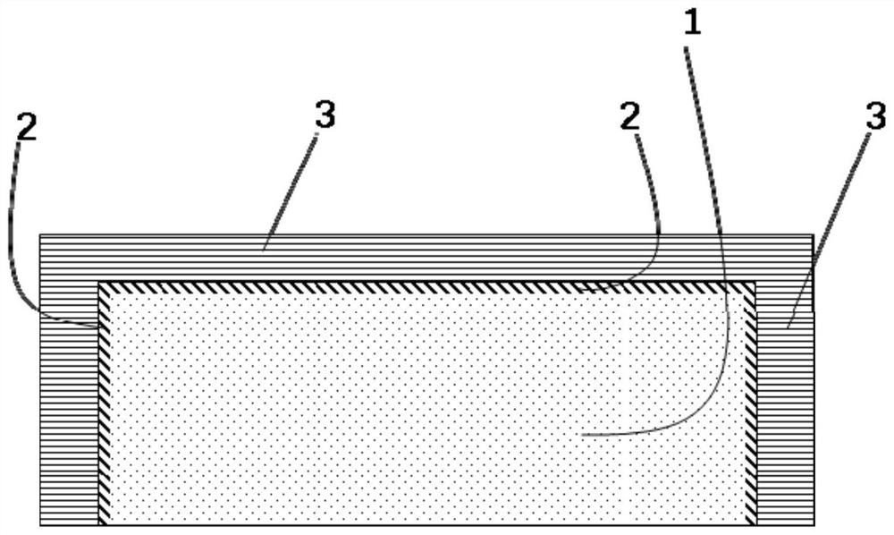
[0042] like figure 1 As shown, in Embodiment 1 of the present invention, the solid medium used for the filter includes a solid medium body 1, and also includes a conductor structure arranged on the surface of the solid medium body, and the conductor structure includes at least one for signal transmission. The first conductive metal layer 2 and the second conductive metal layer 3 for the surface soldering layer; the first conductive metal layer 2 is located on the surface of the solid dielectric body 1; the second conductive metal layer 3 is located on the first conductive metal layer 2 surface; the first conductive metal layer 2 and the second conductive metal layer 3 are conductive layers of different metal materials.

[0043] The surface metallization process of the above-mentioned solid medium, including

[0044] Solid medium body surface treatment step: Since the surface of the sintered solid medium will form a dense polished surface, which is not conducive to the combina...

Embodiment 2

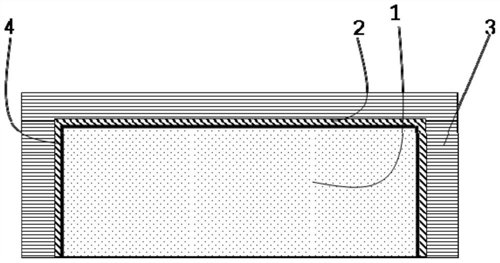
[0058] In Embodiment 2 of the present invention, on the basis of Embodiment 1, further, the conductor structure further includes a third conductor metal layer 4, and the third conductor metal layer 4 is located between the solid dielectric body 1 and the first Between the conductive metal layer 2. In the present invention, the third conductive metal layer is firstly covered on the surface of the solid medium as a transition layer, and then the surface is sintered by screen printing sintering method, electrosilver method, LTCC method, vacuum evaporation method and magnetron sputtering method. A method described herein forms a first conductive metal layer. The purpose of the third conductive metal layer is to enhance the adhesion between the first conductive metal layer for signal transmission and the solid medium. The third conductor metal layer is used as a transition layer. The transition layer connects the solid medium and the first conductor metal layer. The metal material...

Embodiment 3

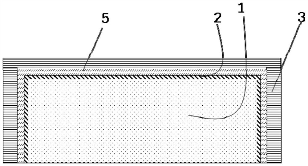
[0069] In Embodiment 3 of the present invention, on the basis of Embodiment 1 above, further, the conductor structure further includes a fourth conductor metal layer 5, and the fourth conductor metal layer 5 is located on the first conductor metal layer 2 and the second conductive metal layer 3.

[0070] Surface metallization process of solid media, including

[0071] Solid medium body surface treatment step: Since the surface of the sintered solid medium will form a dense polished surface, which is not conducive to the combination of the solid medium and the metal layer, it is necessary to roughen the surface of the sintered solid medium in this step Grinding treatment, roughening treatment can adopt the sandpaper of mesh number 150-500 to polish; Then the solid medium after surface roughening is cleaned, removes surface impurity and chemical substance, can take directly to use chemical reagent in the present invention (such as ethanol, deionized water) for rinsing, and etha...


PUM

PropertyMeasurementUnit
thicknessaaaaaaaaaa
thicknessaaaaaaaaaa
thicknessaaaaaaaaaa

Abstract

The invention discloses a solid medium for a filter, which includes a solid medium body, and is characterized in that it also includes a conductor structure arranged on the surface of the solid medium body, and the conductor structure at least includes a first A conductive metal layer and a second conductive metal layer for the surface soldering layer; the first conductive metal layer is located on the surface of the solid medium body; the second conductive metal layer is located on the surface of the first conductive metal layer; the first conductive metal layer layer and the second conductor metal layer are conductor layers of different metal materials. The invention also discloses a solid medium surface metallization process and a dielectric filter. The solid medium of the present invention realizes the replacement of various metals by setting a multi-layer conductor layer structure, reduces the cost and protects the conductor layer actually used for signal transmission from damage, thereby ensuring the signal transmission performance of the solid medium.

Description

technical field [0001] The invention relates to the technical field of communication, in particular to a solid medium used for a filter, its surface metallization process and a dielectric filter. Background technique [0002] Wireless mobile communication base stations are an important physical support for modern communication systems. In order to filter or delete specific frequency signals in the communication process, each base station in the communication network is required to have strong signal processing capabilities to ensure that signal transmission does not appear to be distorted. Microwave filter is a key device for signal processing in base stations, and the improvement of its performance determines the improvement of communication quality and the development direction of communication technology. At present, the miniaturization of filters is one of the key technologies for the development of wireless communication base stations, and the solid dielectric body with...

Claims


Application Information

Patent Timeline
Patent Type & Authority Patents(China)
IPC IPC(8): H01P1/20H01P11/00
CPCH01P1/2002H01P11/007
Inventor 庞新锋伍隽闫松凌蒋金瑞闵祥会苏柯铭
Owner 上海德门信息技术有限公司
Why Eureka
Try Eureka