Preparation method of heterogeneous integrated monocrystal diamond film

A diamond and single crystal technology, which is applied in semiconductor/solid-state device manufacturing, electrical components, circuits, etc., can solve the problems of poor crystal quality, many diamond film defects, and difficult processing, etc., and achieve the effect of high single crystal quality

Inactive Publication Date: 2020-04-07
SHANGHAI INST OF MICROSYSTEM & INFORMATION TECH CHINESE ACAD OF SCI
View PDF4 Cites 5 Cited by
  • Summary
  • Abstract
  • Description
  • Claims
  • Application Information

AI Technical Summary

Problems solved by technology

However, since the growth substrate of the homoepitaxially grown diamond film is a diamond body material, it will face a series of problems such as difficult processing due to the thick substrate, and poor light field mode-locking effect caused by the homogeneity of the film and the substrate.
However, epitaxial growth based on heterogeneous substrates, due to lattice mismatch and thermal matching, results in many defects in the grown diamond film and poor crystal quality, which seriously affects device performance.

Method used


Image

  • Preparation method of heterogeneous integrated monocrystal diamond film
  • Preparation method of heterogeneous integrated monocrystal diamond film
  • Preparation method of heterogeneous integrated monocrystal diamond film

Examples


Embodiment 1

[0061] Such as Figure 1-9 As shown, this embodiment provides a method for preparing a heterogeneously integrated single-crystal graphene film.

[0062] see figure 1, the preparation method of the heterogeneously integrated single-crystal graphene film provided in this embodiment at least includes the following steps:

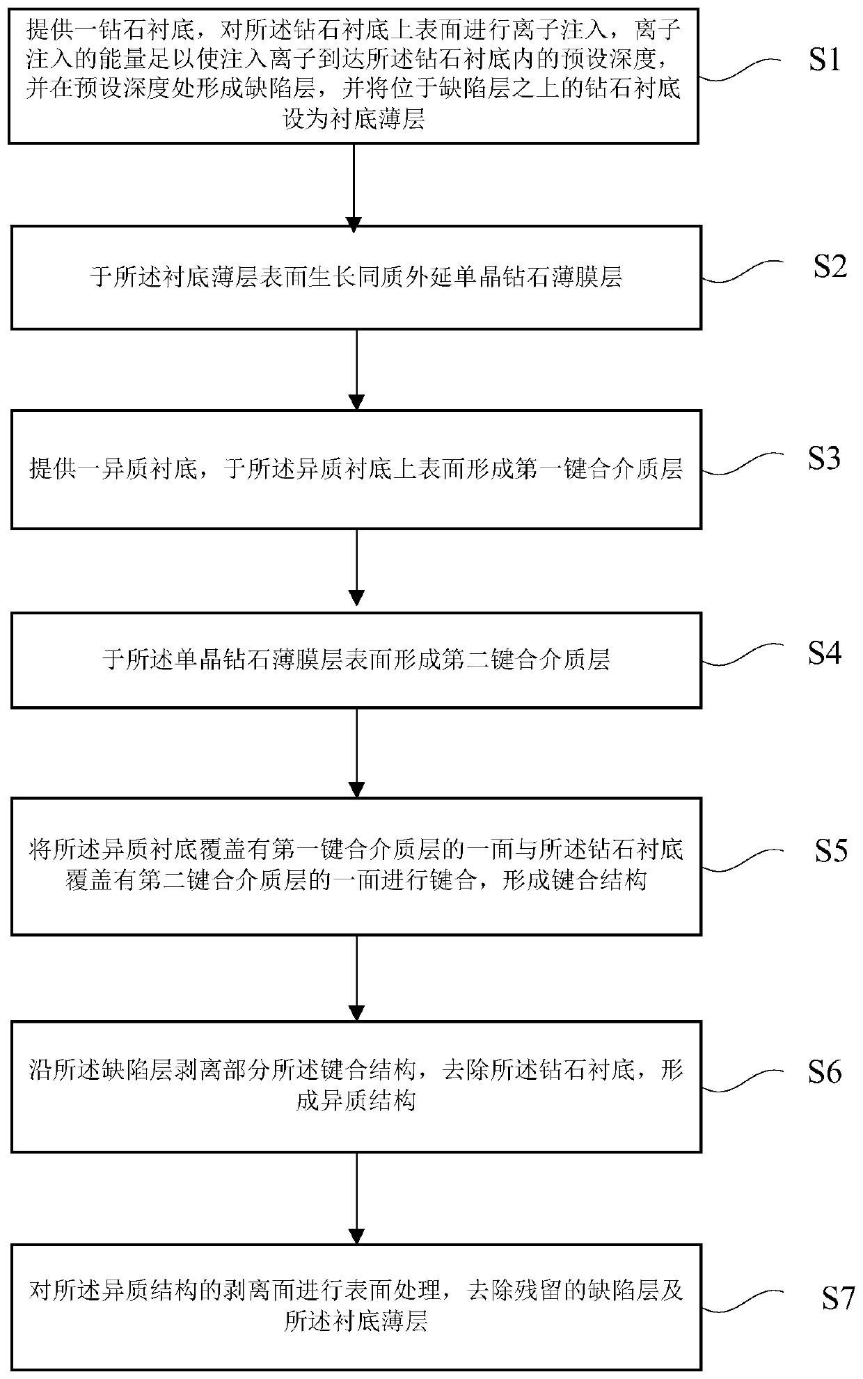
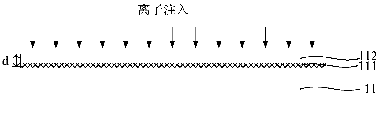
[0063] S1: Provide a diamond substrate, perform ion implantation on the upper surface of the diamond substrate, the energy of the ion implantation is sufficient to make the implanted ions reach a preset depth in the diamond substrate, form a defect layer at the preset depth, and The diamond substrate above the defect layer is set as a substrate thin layer;

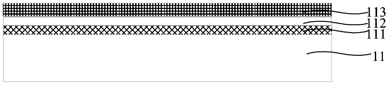
[0064] S2: growing a homoepitaxial single crystal diamond film layer on the surface of the diamond substrate thin layer;

[0065] S3: forming a first bonding medium layer on the surface of the single crystal diamond thin film layer;

[0066] S4: providing a heterogeneous substrate, forming a second bond...

Embodiment 2

[0087] Such as Figures 10-18 As shown, this embodiment provides a method for preparing a heterogeneously integrated single-crystal graphene film,

[0088] see Figure 10 , the present embodiment provides a method for preparing a heterogeneously integrated single crystal diamond thin film, comprising the following steps:

[0089] S1: Provide a diamond substrate, perform ion implantation on the upper surface of the diamond substrate, the energy of the ion implantation is sufficient to make the implanted ions reach a preset depth in the diamond substrate, form a defect layer at the preset depth, and The diamond substrate above the defect layer is set as a substrate thin layer;

[0090] S2: forming a first bonding medium layer on the upper surface of the diamond substrate;

[0091] S3: providing a heterogeneous substrate, forming a second bonding medium layer on the upper surface of the heterogeneous substrate;

[0092] S4: bonding the side of the diamond substrate covered wi...


PUM

PropertyMeasurementUnit
thicknessaaaaaaaaaa
thicknessaaaaaaaaaa
melting pointaaaaaaaaaa

Abstract

The invention relates to a preparation method of a heterogeneous integrated monocrystal diamond film. The preparation method at least comprises the following steps: providing a diamond substrate, carrying out ion implantation on the upper surface of the diamond substrate, forming a defect layer at a preset depth, and setting the diamond substrate on the defect layer as a substrate thin layer; growing a homogeneous epitaxial diamond film layer on the surface of the substrate thin layer; forming a first bonding dielectric layer on the surface of the diamond film layer; providing a heterogeneoussubstrate, and forming a second bonding dielectric layer on the upper surface of the heterogeneous substrate; bonding the first bonding dielectric layer and the second bonding dielectric layer to forma bonding structure; stripping the bonding structure along the defect layer to form a heterostructure; and performing surface treatment on the stripping surface of the heterostructure to remove the residual defect layer and the substrate thin layer. According to the method, the homoepitaxy monocrystal diamond film is integrated on the heterogeneous substrate through the ion implantation and bonding process, the large-area and high-quality diamond film is obtained, and an advanced material platform is provided for photon and quantum sensing device application.

Description

technical field [0001] The invention belongs to the field of preparation of functional materials, in particular to a method for preparing a heterogeneously integrated single crystal diamond film. Background technique [0002] Diamond is a wide bandgap semiconductor with a bandgap of 5.47eV at room temperature, high refractive index, high thermal conductivity, and excellent mechanical and chemical properties. The Mohs hardness of single crystal diamond is 10, which is the hardest material known to exist in nature, with a density of 3.52g / cm 2 , the refractive index is 2.41. Single crystal diamond has a face-centered cubic structure, and each C atom is sp 3 Hybridization forms covalent bonds with the other 4 adjacent C atoms, and every 4 C atoms form a regular tetrahedron, so macroscopically natural diamonds tend to be regular octahedrons. The C-C bond in diamond is very strong, and there are no free electrons, which leads to high hardness and high chemical stability of dia...

Claims


Application Information

Patent Timeline
Patent Type & Authority Applications(China)
IPC IPC(8): H01L21/78H01L21/762H01L21/265
CPCH01L21/7813H01L21/26506H01L21/76254H01L2021/26573
Inventor 欧欣伊艾伦武震宇
Owner SHANGHAI INST OF MICROSYSTEM & INFORMATION TECH CHINESE ACAD OF SCI
Why Eureka
Try Eureka