
Method for preparing nickel-vanadium sputtering target material

A sputtering target, nickel-vanadium technology, applied in the field of nickel-vanadium sputtering target preparation, to achieve the effect of compact structure without pores, fine and uniform grains, and high sputtering efficiency

Active Publication Date: 2020-04-14
GRIKIN ADVANCED MATERIALS +1
View PDF4 Cites 5 Cited by
  • Summary
  • Abstract
  • Description
  • Claims
  • Application Information

AI Technical Summary

Problems solved by technology

At present, there is no complete process for preparing nickel-vanadium sputtering targets with uniform and fine microstructure in the industry. It is urgent to design a nickel-vanadium sputtering target preparation process to meet customer and market requirements.

Method used


Image

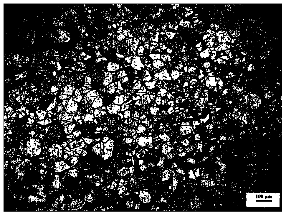
  • Method for preparing nickel-vanadium sputtering target material
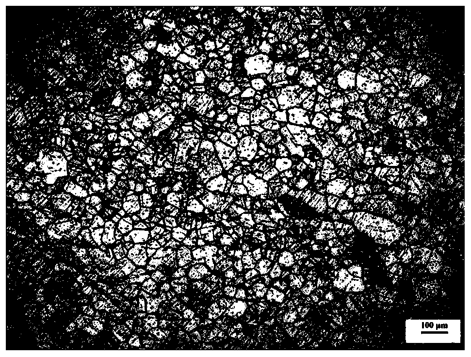
  • Method for preparing nickel-vanadium sputtering target material
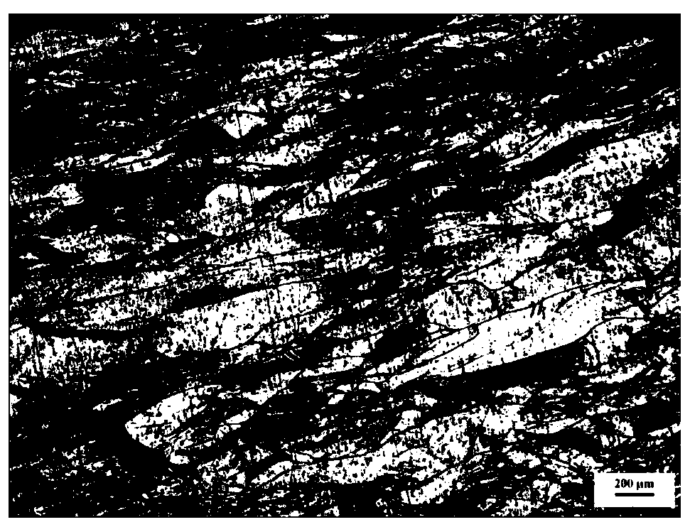
  • Method for preparing nickel-vanadium sputtering target material

Examples


Embodiment 1

[0019] The purity of raw materials is 99.95% (3N5) The nickel vanadium ingot carries out the following process steps:

[0020] Step 1) hot forging the nickel vanadium ingot. The holding temperature before hot forging is 1250±50°C, and the holding time is 1h-2h. After being out of the furnace, the nickel-vanadium ingot is roughly drawn and lengthened along the axial pier for more than 3 times, and air-cooled after the forging is completed;

[0021] Step 2) annealing the blank of step 1). The annealing temperature is 850±50°C, and the annealing time is 1-2h.

[0022] Step 3) rolling and deforming the billet in step 2). The total cold deformation rate is 85±5%, and the cold deformation method is cross rolling, wherein the rolling pass deformation is controlled at 7-15%.

[0023] Step 4) Perform annealing treatment on the billet of step 3), the annealing temperature is 900°C±50°C, and the annealing time is 1-2h.

[0024] Sampling and analyzing the microstructure of the bill...

Embodiment 2

[0026] The purity of raw materials is 99.95% (3N5) The nickel vanadium ingot carries out the following process steps:

[0027] Step 1) hot forging the nickel vanadium ingot. The holding temperature before hot forging is 950±50°C, and the holding time is 3h-4h. After being out of the furnace, the nickel-vanadium ingot is roughly drawn and lengthened along the axial pier for more than 3 times, and air-cooled after the forging is completed;

[0028] Step 2) annealing the blank of step 1). The annealing temperature is 950±50°C, and the annealing time is 1-2h.

[0029] Step 3) rolling and deforming the billet in step 2). The total cold deformation rate is 70±5%, and the cold deformation method is cross rolling, wherein the rolling pass deformation is controlled at 7-15%.

[0030] Step 4) Perform annealing treatment on the billet of step 3), the annealing temperature is 700°C±50°C, and the annealing time is 2-3h.

[0031] Sampling and analyzing the microstructure of the bille...


PUM

PropertyMeasurementUnit
crystal sizeaaaaaaaaaa

Abstract

The invention belongs the technical field of metal material processing and microelectronic material manufacturing, and discloses a method for preparing a nickel-vanadium sputtering target material. The method for preparing the nickel-vanadium sputtering target material includes the steps that a nickel-vanadium ingot is sequentially subjected to (1) hot forging, (2) annealing, (3) cold deformation,and (4) secondary annealing. The content of V in the nickel-vanadium sputtering target material is 7 + / - 0.7%, and the purity of the nickel-vanadium ingot is 99.9% to 99.995%. The crystal grain sizeof the obtained nickel-vanadium sputtering target material is less than or equal to150 [mu]m, the crystal grains are fine, and distribution is uniform. The nickel-vanadium sputtering target material has high purity of above 99.9%; the organizational structure is dense without pores, the crystal grains are fine and uniform, the crystal grain size is less than or equal to 150 [mu]m, non-magnetic effect is achieved, the sputtering efficiency is high, and the method can be widely applied to electronic components, communications, solar photovoltaics and other industries.

Description

technical field [0001] The invention belongs to the technical field of metal material processing and microelectronic material manufacturing, and in particular relates to a method for preparing a nickel-vanadium sputtering target. Background technique [0002] Sputtering targets are commonly used to prepare conductive, bonding and barrier metals in integrated circuits. Because conductive layer metals such as gold and silver react easily with silicon wafers to form low-melting point compounds, resulting in weak interface bonding, it is generally necessary to use pure nickel as a bonding layer to prevent it. However, the pure nickel bonding layer will still diffuse with the wire layer metal, so a barrier layer is needed to prevent diffusion. Generally, pure vanadium is used as the barrier layer material. The nickel-vanadium sputtering target is made by adding vanadium to the nickel melt, which combines the advantages of the nickel target and the vanadium target, and can comple...

Claims


Application Information

Patent Timeline
Patent Type & Authority Applications(China)
IPC IPC(8): C22F1/10C22C19/03C23C14/34
CPCC22C19/03C22F1/10C23C14/3414
Inventor 郭姗姗曾浩张巧霞王焕焕万小勇陈畅李勇军陈明
Owner GRIKIN ADVANCED MATERIALS
Learn More