Two-dimensional traveling wave high-gain broadband CMOS power amplifier

A power amplifier, high gain technology, used in power amplifiers, amplifiers, amplifiers with semiconductor devices/discharge tubes, etc., can solve the problems of reduced output power characteristics, low ultra-wideband gain, power characteristics deterioration, etc., to simplify the series connection. The effect of voltage divider structure, high power output capability, and simple power supply network

Pending Publication Date: 2020-04-17
QINGHAI UNIV FOR NATITIES
View PDF0 Cites 2 Cited by
  • Summary
  • Abstract
  • Description
  • Claims
  • Application Information

AI Technical Summary

Problems solved by technology

[0003] (1) Limited broadband high-gain amplification capability: Traditional single transistors are affected by the gain-bandwidth product, and gain must be sacrificed to obtain ultra-wideband amplification capability. Therefore, the wideband high-gain amplification capability is severely limited
[0004] (2) Broadband high power amplification capability is limited: the characteristic frequency of transistors in semiconductor processes is getting higher and higher, which brings low breakdown voltage and limits the power capacity of a single transistor
[0006] ①In the traditional distributed power amplifier, the core amplifier circuit is realized by a distributed amplification arrangement of multiple single transistors. Since the single transistor is affected by parasitic parameters, its power gain will be significantly reduced as the operating frequency increases. , At the same time, the power characteristics will be significantly deteriorated, so in order to obtain an ultra-wideband flat amplification structure, it is necessary to sacrifice low-frequency gain to balance high-frequency loss, resulting in very low ultra-wideband gain of traditional distributed amplifiers;
[0007] ②In order to improve the amplifier gain and improve the isolation, there are also Cascode dual-transistor distributed amplification structures. However, although the Cascode dual-transistor increases the circuit isolation, it cannot gain a significant deterioration with frequency, nor can it realize the Cascode dual-transistor. Optimum impedance matching, which reduces output power characteristics
[0008] It can be seen from this that the design difficulties of ultra-wideband RF power amplifiers based on integrated circuit technology are: high power output under ultra-wideband is difficult; the traditional single transistor structure or the distributed amplification structure of Cascode transistors have many limitations

Method used


Image

  • Two-dimensional traveling wave high-gain broadband CMOS power amplifier
  • Two-dimensional traveling wave high-gain broadband CMOS power amplifier

Examples


Embodiment Construction

[0035] Exemplary embodiments of the present invention will now be described in detail with reference to the accompanying drawings. It should be understood that the implementations shown and described in the drawings are only exemplary, intended to explain the principle and spirit of the present invention, rather than limit the scope of the present invention.

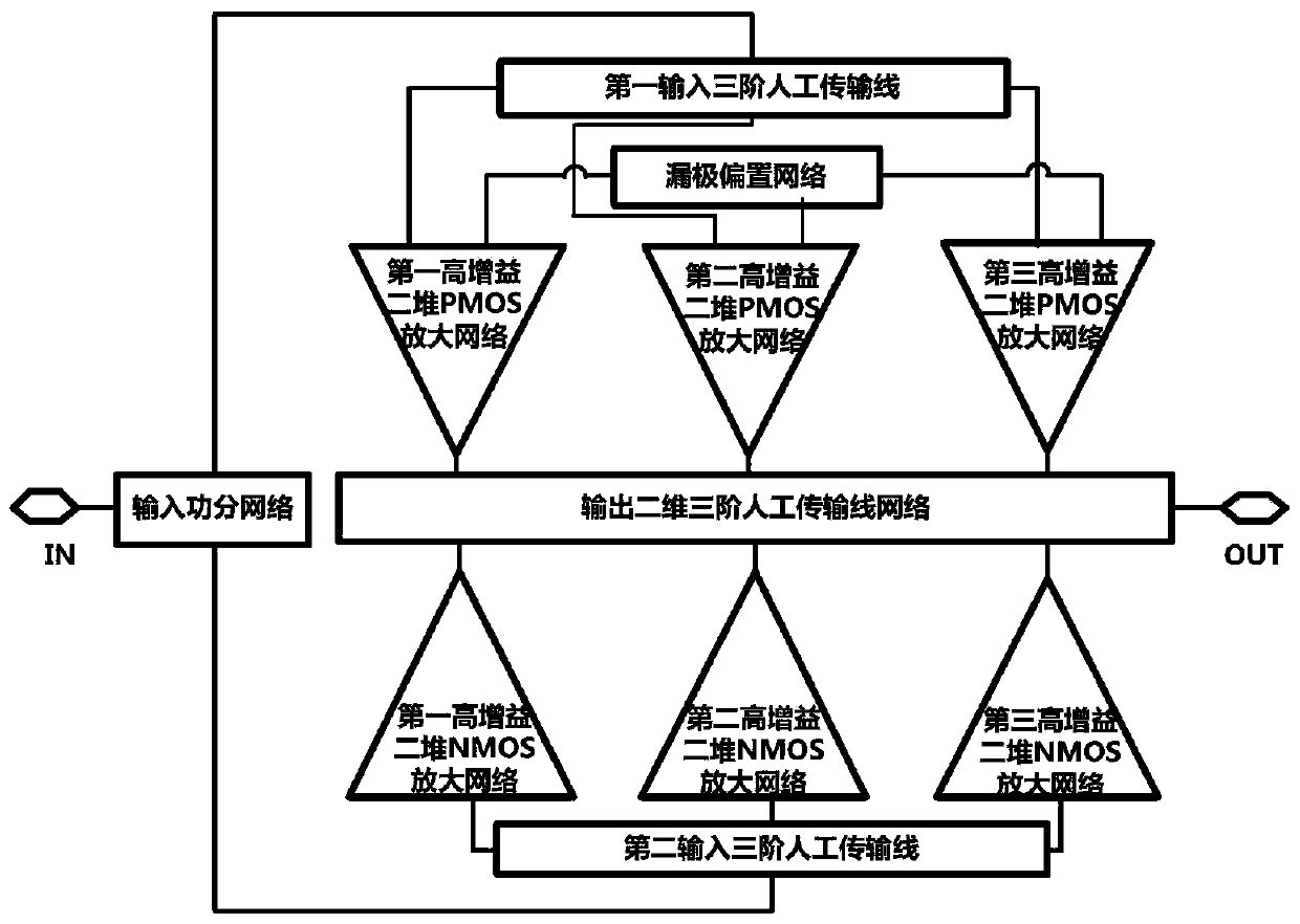
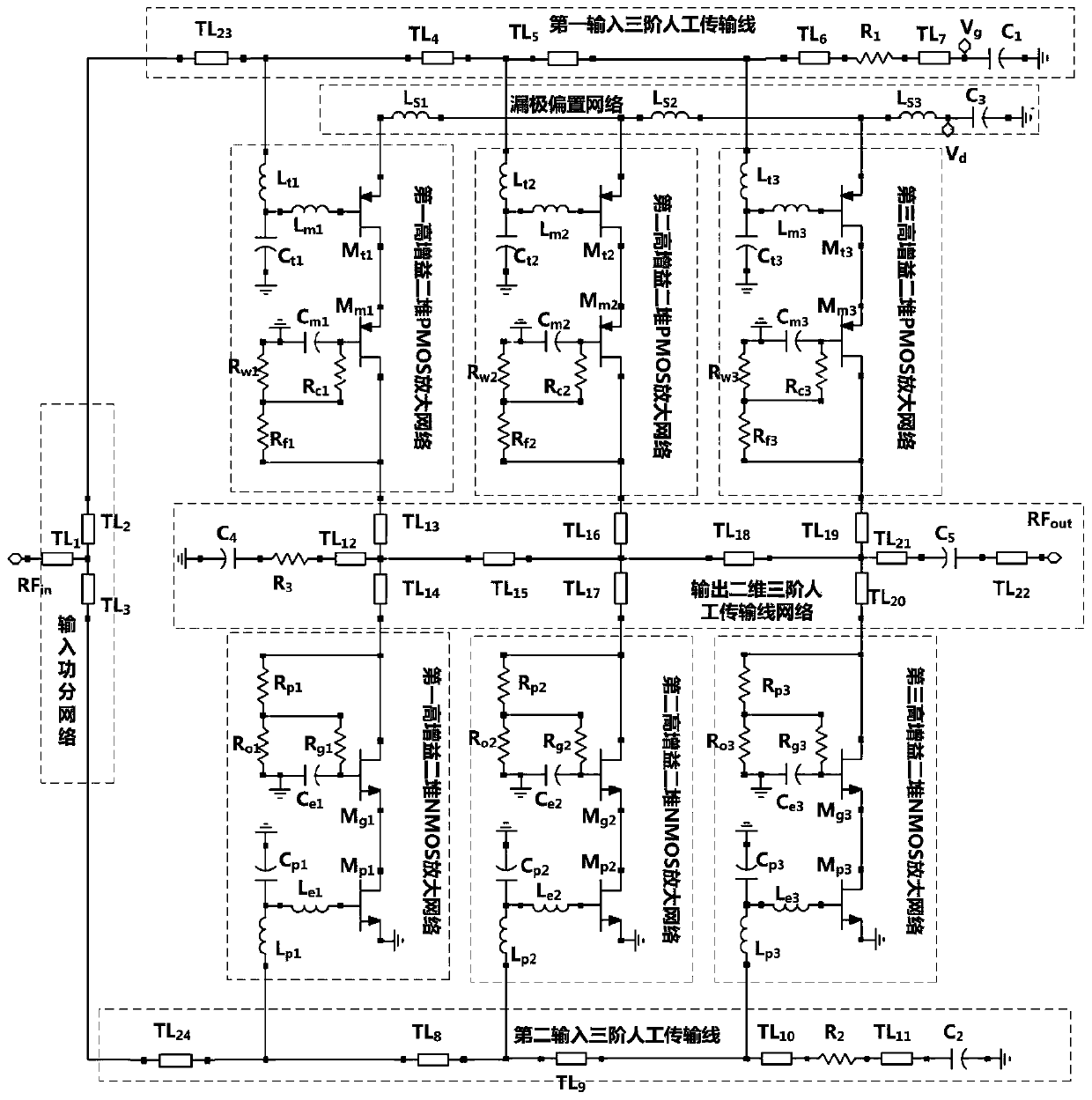
[0036] An embodiment of the present invention provides a two-dimensional traveling wave high-gain broadband CMOS power amplifier, which is characterized in that it includes an input power division network, a first input third-order artificial transmission line, a second input third-order artificial transmission line, a drain bias network, The first high-gain two-stack PMOS amplifying network, the second high-gain two-stack PMOS amplifying network, the third high-gain two-stack PMOS amplifying network, the first high-gain two-stack NMOS amplifying network, the second high-gain two-stack NMOS amplifying network, The third ...


PUM


Abstract

The invention discloses a two-dimensional traveling wave high-gain broadband CMOS power amplifier, which comprises an input power division network, a first input third-order artificial transmission line, a second input third-order artificial transmission line, a drain bias network, a first high-gain two-pile PMOS amplification network, a second high-gain two-pile PMOS amplification network, a third high-gain two-pile PMOS amplification network, a first high-gain two-pile NMOS amplification network, a second high-gain two-pile NMOS amplification network, a third high-gain two-pile NMOS amplification network and an output two-dimensional three-order artificial transmission line network. The core architecture adopts the characteristics of high power and high gain of the high-gain two-pile PMOS and NMOS amplification networks in the microwave band, and meanwhile, the ultra-wideband frequency response characteristic and the simplified series voltage division structure of the two-dimensionaltraveling wave amplifier structure are utilized, so that the whole power amplifier obtains good wideband, high gain, high efficiency and high power output capability, and a power supply network is simple.

Description

technical field [0001] The invention relates to field effect transistor radio frequency power amplifiers and the field of integrated circuits, in particular to a two-dimensional traveling wave high-gain broadband CMOS power amplifier applied to a transmitting module at the end of a radio frequency microwave transceiver. Background technique [0002] With the rapid development of wireless communication systems and RF microwave circuits, RF front-end transceivers are also developing in the direction of high performance, high integration, and low power consumption. Therefore, the market urgently needs the radio frequency and microwave power amplifier of the transmitter to have high output power, high gain, high efficiency, low cost and other performances, and the integrated circuit is the key technology that is expected to meet the market demand. However, when using integrated circuit technology to design and implement RF and microwave power amplifier chip circuits, its perform...

Claims


Application Information

Patent Timeline
Patent Type & Authority Applications(China)
IPC IPC(8): H03F1/02H03F1/42H03F3/195H03F3/213H03F3/24H03F3/60
CPCH03F1/0205H03F1/42H03F3/195H03F3/245H03F3/604H03F3/607
Inventor 林倩邬海峰
Owner QINGHAI UNIV FOR NATITIES
Why Eureka
Try Eureka