
Schottky diode and manufacturing method thereof

A Schottky diode and Schottky contact technology, which is applied in semiconductor/solid-state device manufacturing, electrical components, circuits, etc., can solve the problem of low cut-off frequency of Schottky diodes, achieve drive enhancement, increase cut-off frequency, increase Effect of Large Electron Concentration

Inactive Publication Date: 2020-04-21
SUN YAT SEN UNIV
View PDF9 Cites 1 Cited by
  • Summary
  • Abstract
  • Description
  • Claims
  • Application Information

AI Technical Summary

Problems solved by technology

At present, due to the limitation of the thickness of the two-dimensional electron gas, the single-channel Schottky diode has the problem of low cut-off frequency of the Schottky diode.

Method used


Image

  • Schottky diode and manufacturing method thereof
  • Schottky diode and manufacturing method thereof
  • Schottky diode and manufacturing method thereof

Examples


Embodiment Construction

[0036] The following will clearly and completely describe the technical solutions in the embodiments of the present invention with reference to the accompanying drawings in the embodiments of the present invention. Obviously, the described embodiments are only some, not all, embodiments of the present invention. Based on the embodiments of the present invention, all other embodiments obtained by persons of ordinary skill in the art without making creative efforts belong to the protection scope of the present invention.

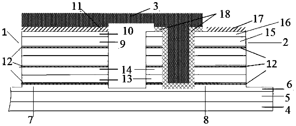
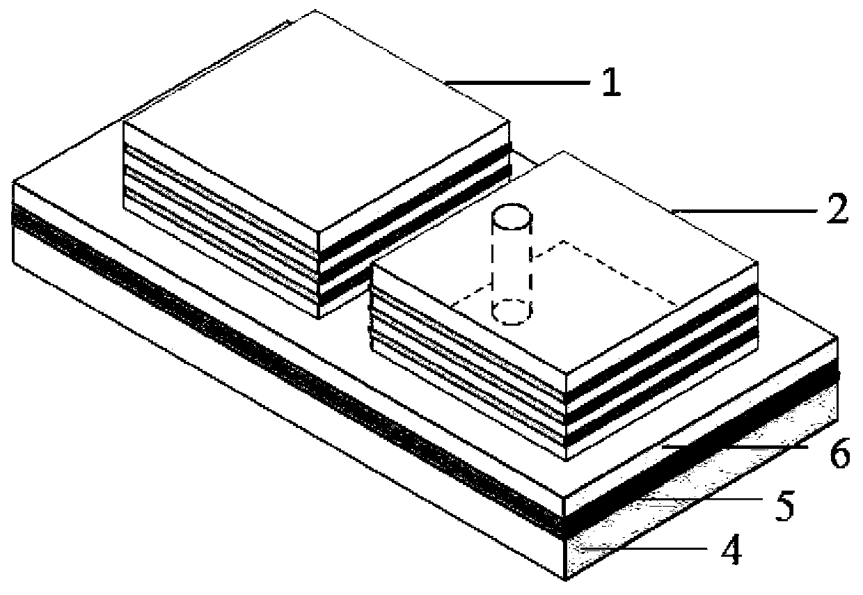
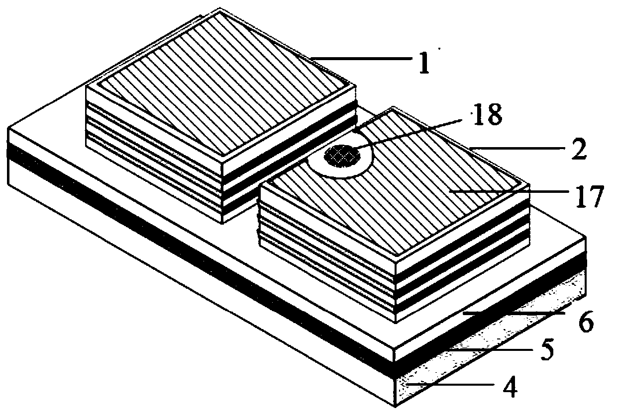
[0037] The object of the present invention is to provide a Schottky diode and a preparation method thereof. The present invention increases the electron concentration in the longitudinal range of the diode by increasing the thickness of the two-dimensional electron gas in the longitudinal range of the diode, so that the drive of the lateral electron flow is enhanced, effectively The channel resistance is reduced; the Schottky contact metal evaporation position ...


PUM


Abstract

The invention discloses a Schottky diode and a manufacturing method thereof. The Schottky diode comprises a substrate layer, a first convex body, a second convex body and an air bridge. The first convex body and the second convex body are arranged on the substrate layer and connected through the air bridge. The first convex body and the second convex body are provided with a plurality of two-dimensional electron gas layers; and a two-dimensional electron gas thickness in a longitudinal range of the diode is increased, an electron concentration in the longitudinal range of the diode is increased too, a limitation of the thickness of a single-channel two-dimensional electron gas is broken through, transverse electron flow driving is enhanced, a channel resistance is effectively reduced, anda cut-off frequency of the Schottky diode is improved. According to the Schottky diode, a through cavity is etched in a Schottky contact metal evaporation position, and Schottky contact metal is connected with the two-dimensional electron gas of all channel layers through the through cavity so that a current does not need to pass through a barrier layer, the resistance of the barrier layer is reduced, a series resistance of the device is decreased, and the higher cut-off frequency can be obtained.

Description

technical field [0001] The invention relates to the technical field of terahertz frequency bands of semiconductor chips, in particular to a Schottky diode and a preparation method thereof. Background technique [0002] Because the Schottky diode has the advantages of fast speed, good nonlinear effect, ability to work at room temperature, and easy integration, when the cut-off frequency of the Schottky diode reaches terahertz, it can achieve frequency doubling or mixing of high-frequency signals. frequency, so they are often used as mixers and detector diodes in terahertz detectors. [0003] Due to the large difference in the energy gap of III-nitride materials, from 0.7eV of InN, 3.4eV of GaN to 6.2eV of AlN, there is a huge energy band shift in the conduction band of the heterojunction interface, coupled with its strong polarization-induced Therefore, group III nitride materials are currently the semiconductor material systems that can provide the highest two-dimensional e...

Claims


Application Information

Patent Timeline
IPC IPC(8): H01L29/872H01L29/06H01L21/329
CPCH01L29/0603H01L29/0684H01L29/66143H01L29/872
Inventor 张佰君姚婉青柳月波
Owner SUN YAT SEN UNIV
Features
  • Generate Ideas
  • Intellectual Property
  • Life Sciences
  • Materials
  • Tech Scout
  • Unparalleled Data Quality
  • Higher Quality Content
  • 60% Fewer Hallucinations
Learn More