Ultraviolet photoelectric device and preparation method thereof
A technology of electrical devices and ultraviolet light, applied in photovoltaic power generation, electrical components, semiconductor devices, etc., can solve the problems of low hole transport efficiency and strong ultraviolet absorption
- Summary
- Abstract
- Description
- Claims
- Application Information
AI Technical Summary
Problems solved by technology
Method used
Image
Examples
no. 1 example
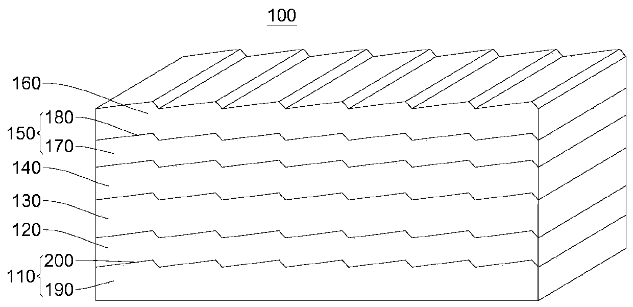
[0033] see figure 1 with figure 2 , the present embodiment provides an ultraviolet optoelectronic device 100, the ultraviolet optoelectronic device 100 includes a substrate 110 and a substrate 120 sequentially grown on the substrate 110, an n-type AlGaN layer 130, an active region 140, a p-type AlGaN layer 150 and contact layer 160. Wherein, the p-type AlGaN layer 150 includes a first body 170 and a first step 180 located on the top surface of the first body 170, a plurality of first steps 180 are periodically arranged in sequence, and the vertical height of the first step 180 is Straight section is triangular.
[0034] The drop distance L between two adjacent first steps 180 is greater than the thickness of the monoatomic layer. The drop distance L between two adjacent first steps 180 refers to the distance between the top surfaces of two adjacent first steps 180 , and of course the top surfaces of two adjacent first steps 180 are parallel to each other. It can also be s...
no. 2 example
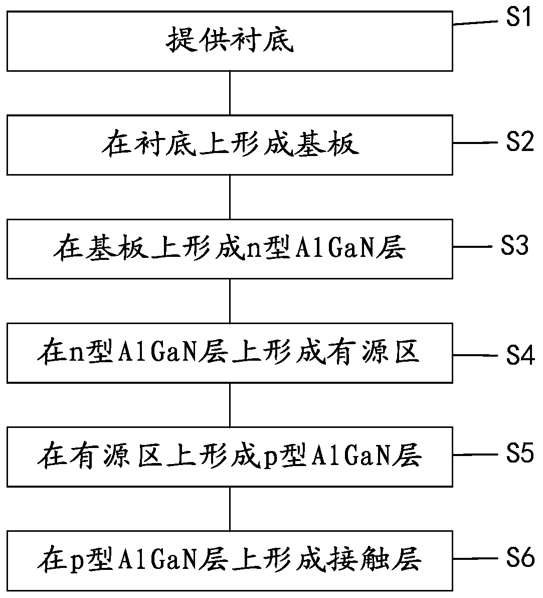
[0044] see image 3 , this embodiment provides a method for manufacturing the ultraviolet photoelectric device 100, which is mainly used for preparing the ultraviolet photoelectric device 100 in the first embodiment. The preparation method includes sequentially growing a substrate 120, an n-type AlGaN layer 130, an active region 140 and a p-type AlGaN layer 150 on a substrate 110; wherein the p-type AlGaN layer 150 includes a first body 170 and is located at the second For the first steps 180 on the top surface of a body 170 , the drop distance L between two adjacent first steps 180 is greater than the thickness of a monoatomic layer.
[0045] Specifically, the following steps are included:
[0046] S1: providing a substrate 110 .
[0047] The material of the substrate 110 is sapphire, and the substrate 110 is placed in the reaction chamber of the growth equipment. The growth equipment can be any one of metal-organic chemical vapor deposition, hydride vapor deposition, and m...
PUM
 Abstract
Description
Claims
Application Information


