Device and method for testing dielectric properties of solid insulating material interface

A technology of solid insulating materials and dielectric properties, applied in the direction of dielectric property measurement, measuring devices, testing dielectric strength, etc., can solve the problems of large cake-shaped materials, large test devices, uneven electric field distribution, etc., to achieve Good insulation and shielding effect, simple test method, stable and adjustable temperature effect

Active Publication Date: 2021-03-05
ZHEJIANG UNIV +1
View PDF12 Cites 0 Cited by
  • Summary
  • Abstract
  • Description
  • Claims
  • Application Information

AI Technical Summary

Problems solved by technology

Different types of insulating materials with different dielectric properties contact to form a solid-solid interface. Due to the uneven distribution of the electric field at the material interface, there is field strength distortion. The insulation strength of the solid interface is much lower than that of the cable insulation body, and the installation of field joints is usually It is carried out in a non-clean room and uncontrolled environmental conditions, which makes it easy to form tiny defects (such as air gaps, dust, pollutants and other impurities) at the joint interface, resulting in insulation failure
[0004] For the current research on the interface problem of cable joints, Emre Kantar et al. designed a flat electrode, which is pressured by a heavy object, and the electrode is immersed in transformer oil as a whole. The breakdown characteristics of the interface under different roughness and pressure have been studied, but there is no temperature. Related research, and the test device is large in size. When the pressure reaches 1.16MPa, the required weight has reached 26kg. If the pressure is increased again, the operation is relatively difficult and there are certain safety risks.
Zhu et al. changed the shape of the test material, used a cake-shaped material, placed a thin ring electrode between the two materials, and studied the interface characteristics under different roughness and pressure, but did not involve the relevant research on temperature, and the design The volume of the medium cake material is relatively large, and a certain thickness of electrode material is introduced at the interface. The test results are not real and effective material interface characteristics.

Method used


Image

  • Device and method for testing dielectric properties of solid insulating material interface
  • Device and method for testing dielectric properties of solid insulating material interface
  • Device and method for testing dielectric properties of solid insulating material interface

Examples


example 1

[0054] Example 1, interface conductivity test, comprising the following steps:

[0055] Step 1: Prepare the sample.

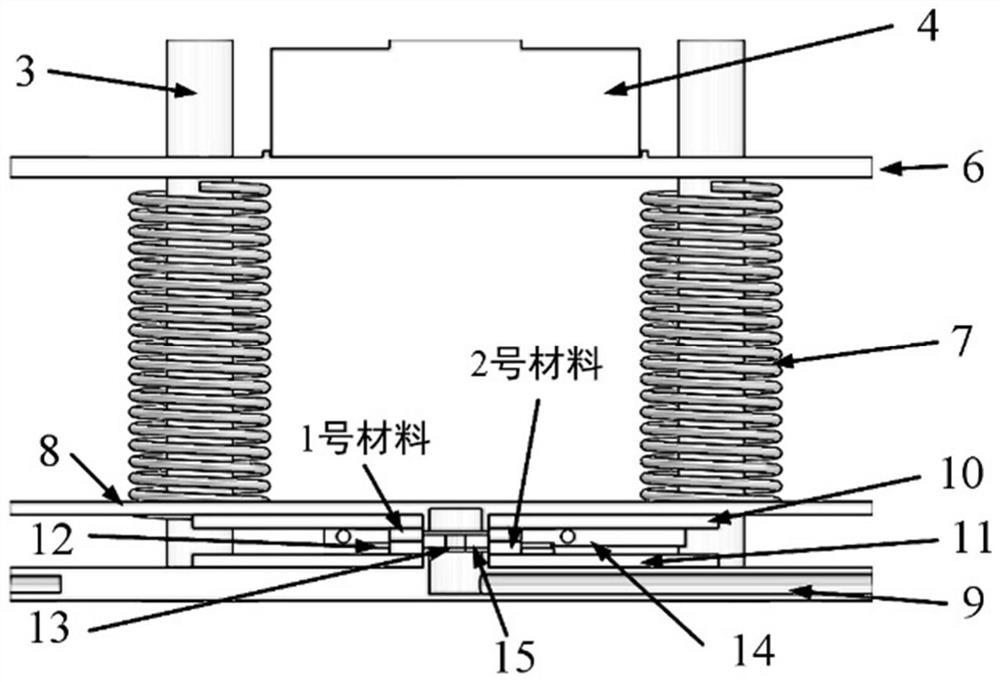
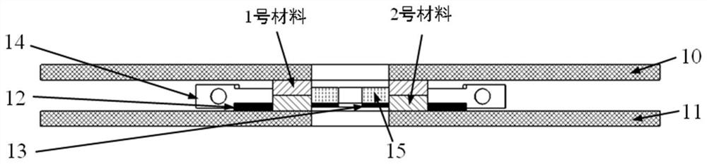
[0056] Samples No. 1 and No. 2 were prepared from cross-linked polyethylene (XLPE). Samples No. 1 and No. 2 were circular rings of the same size, with an inner diameter of 10 mm, an outer diameter of 14 mm, and a thickness of 3 mm. Purpose Sandpaper is used to polish the surface of materials, and the interface is formed by the contact of two materials.

[0057] Step 2: According to the geometric structure of the material interface, calculate the material interface area, the formula is as follows:

[0058]

[0059] In the formula, π is the circumference ratio, R 2 is the outer radius of the ring material to be tested, R 1 is the inner radius of the ring material to be tested. Material interface area is 0.75cm 2 .

[0060] Step 3: Select 1MPa as the test pressure of the material interface, and calculate the pressure exerted by the pressure control device...

example 2

[0081] Example 2, interface partial discharge test, including the following steps:

[0082] Step 1: Prepare the sample.

[0083] Samples No. 1 and No. 2 were prepared from cross-linked polyethylene (XLPE). Samples No. 1 and No. 2 were circular rings of the same size, with an inner diameter of 10 mm, an outer diameter of 14 mm, and a thickness of 3 mm. Purpose Sandpaper is used to polish the surface of materials, and the interface is formed by the contact of two materials.

[0084] Step 2: According to the geometric structure of the material interface, calculate the material interface area, the formula is as follows:

[0085]

[0086] In the formula, π is the circumference ratio, R 2 is the outer radius of the ring material to be tested, R 1 is the inner radius of the ring material to be tested. Material interface area is 0.75cm 2 .

[0087] Step 3: Select 1MPa as the test pressure of the material interface, and calculate the pressure exerted by the pressure control de...


PUM

PropertyMeasurementUnit
lengthaaaaaaaaaa
diameteraaaaaaaaaa
thicknessaaaaaaaaaa

Abstract

The invention discloses a device and method for testing the interface dielectric properties of solid insulating materials. The device includes a pressure regulating device, an insulating component and an electrode component; Pressure regulation to provide pressure at the interface for solid materials. The insulating component ensures the insulating performance between the electrode component and the pressure regulating device. The electrode assembly is tightly fitted at the interface between the electrode and the material by means of bolt fastening. During testing, the device was placed in an oven. The invention can effectively suppress the leakage current on the non-interface side of the material, display the pressure indication in real time, is small in size, simple in the test method, convenient in operation, and can test the dielectric properties of the interface of the solid insulating material under different pressures and temperatures.

Description

technical field [0001] The invention belongs to the technical field of high voltage and insulation, in particular to a device and method for testing the interface dielectric properties of solid insulating materials. Background technique [0002] The electric power industry is the basic industry for national economic development and industrialization. With the continuous acceleration of my country's urbanization process and sustained and rapid economic development, the demand for electric power consumption is increasing day by day. In order to effectively reduce the consumption of fossil energy and reduce environmental pollution, the future power system is undergoing a major transformation. Renewable energy such as solar energy and wind energy will become the main source of electricity in two ways: centralized and distributed. With the increasing demand for power supply, power cables have become one of the key power equipment for constructing urban underground energy comprehe...

Claims


Application Information

Patent Timeline
Patent Type & Authority Patents(China)
IPC IPC(8): G01R31/12G01R27/26
CPCG01R27/2694G01R31/1263
Inventor 陈向荣孟繁博贾磊傅明利王婷婷侯帅李瑞显
Owner ZHEJIANG UNIV
Why Eureka
Try Eureka