Monocrystalline silicon wafer processing method, monocrystalline silicon wafer and solar cell

A processing method and technology for single crystal silicon wafers, applied in the field of solar cells, can solve the problem of low conversion effect, etc., and achieve the effects of improving absorption efficiency, improving absorption rate and uniform surface

Active Publication Date: 2020-04-28
BEIJING NORTH HUACHUANG VACUUM TECH CO LTD
View PDF12 Cites 0 Cited by
  • Summary
  • Abstract
  • Description
  • Claims
  • Application Information

AI Technical Summary

Problems solved by technology

[0003] In the prior art, there are a large number of methods for improving the efficiency of solar cells by making texture, but there are still problems such as low conversion effect

Method used


Image

  • Monocrystalline silicon wafer processing method, monocrystalline silicon wafer and solar cell

Examples


preparation example Construction

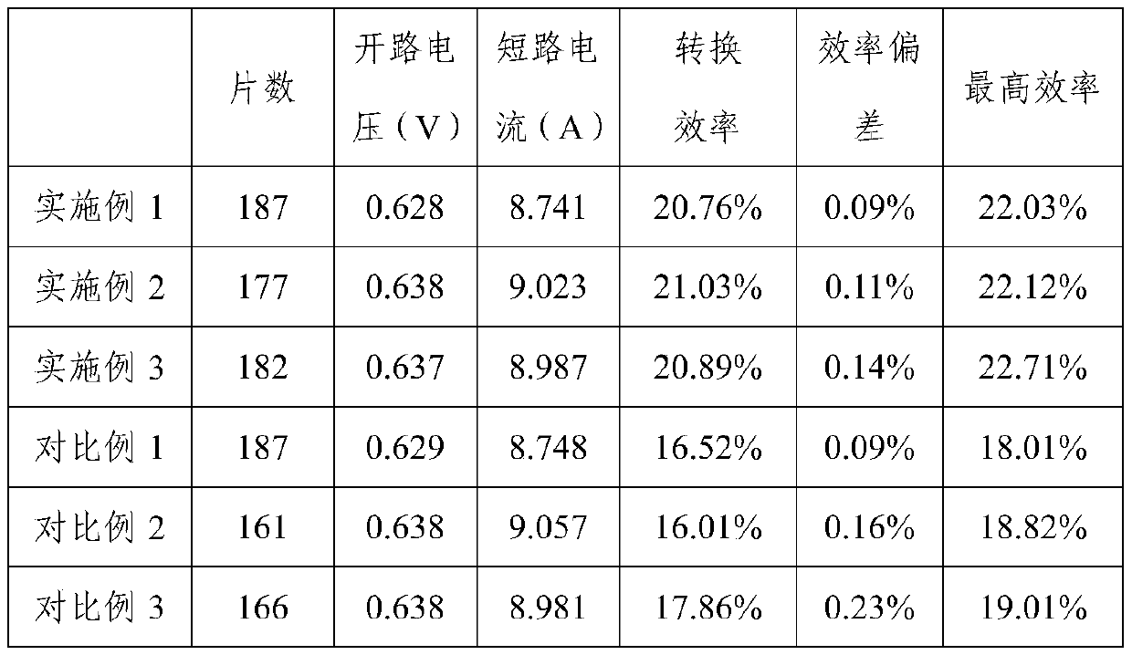
[0051] This embodiment relates to a method for preparing a monocrystalline silicon solar cell, and the processing of a monocrystalline silicon wafer includes the following steps:

[0052]1) Alkali polishing, the cut monocrystalline silicon wafer is polished with a sodium hydroxide solution with a concentration of 4wt%, the polishing temperature is controlled at 60°C, and the polishing time is controlled at 160s to remove the damaged layer of the silicon wafer;

[0053] 2) Pure iron sputtering etching. Firstly, the alkali-polished silicon wafer was washed with deionized water and then dried. Then, it was installed on the target frame as a target material. The pure iron powder sample dish with an average particle size of 60 μm was sputtered. The radiation power is 300W, and the sputtering time is 60min; then, the iron-containing silicon wafer is cleaned with a mixed acid with a hydrochloric acid concentration of 15wt% and a nitric acid concentration of 5wt%, and then cleaned with...

Embodiment 2

[0060] This embodiment relates to a method for preparing a monocrystalline silicon solar cell, and the processing of a monocrystalline silicon wafer includes the following steps:

[0061] 1) Alkali polishing, the cut monocrystalline silicon wafer is polished with a sodium hydroxide solution with a concentration of 2wt%, the polishing temperature is controlled at 60°C, and the polishing time is controlled at 150s to remove the damaged layer of the silicon wafer;

[0062] 2) Pure iron sputtering etching. Firstly, the alkali-polished silicon wafer was washed with deionized water and then dried. Then it was installed on the target frame as a target. The pure iron powder sample dish with an average particle size of 50 μm was sputtered The radiation power is 50W, and the sputtering time is 30min; then, the iron-containing silicon wafer is cleaned with a mixed acid with a hydrochloric acid concentration of 12wt% and a nitric acid concentration of 3wt%, and then cleaned with deionized ...

Embodiment 3

[0070] This embodiment relates to a method for preparing a monocrystalline silicon solar cell, comprising the following steps:

[0071] 1) Alkali polishing, the cut monocrystalline silicon wafer is polished with a sodium hydroxide solution with a concentration of 4wt%, the polishing temperature is controlled at 60°C, and the polishing time is controlled at 160s to remove the damaged layer of the silicon wafer;

[0072] 2) Pure iron sputtering etching. Firstly, the alkali-polished silicon wafer was washed with deionized water and then dried. Then, it was installed on the target frame as a target material. The pure iron powder sample dish with an average particle size of 60 μm was sputtered. The radiation power is 300W, and the sputtering time is 60min; then, the iron-containing silicon wafer is cleaned with a mixed acid with a hydrochloric acid concentration of 15wt% and a nitric acid concentration of 5wt%, and then cleaned with deionized water to remove iron and silicon powder....


PUM

PropertyMeasurementUnit
thicknessaaaaaaaaaa
particle sizeaaaaaaaaaa

Abstract

The invention belongs to the technical field of solar cells, and particularly relates to a monocrystalline silicon wafer processing method, a monocrystalline silicon wafer and a solar cell. Processingof the monocrystalline silicon wafer comprises the following steps: 1) performing primary texturing and primary diffusion preparation on one surface of the monocrystalline silicon wafer to form a p-njunction; 2) performing acid cleaning to remove unstable p-n junctions and unstable suede structures; and 3) performing second texturing and second diffusion on the surface of the monocrystalline silicon wafer. The thickness of the textured structure formed after the second texturing is less than 10 nanometers, so that transmission of sunlight can be realized. According to the invention, throughtwice texturing and twice diffusion, the unit specific surface area of the upper surface of the silicon wafer is increased; and particularly, the textured structure after the second texturing can realize sunlight transmission, so that the light absorption efficiency is improved, the p-n junction obtained after the treatment is more uniform, the p-n junction is prepared into the solar cell, and theobtained cell has higher sunlight absorption efficiency.

Description

technical field [0001] The invention belongs to the technical field of solar cells, and in particular relates to a processing method of a single crystal silicon chip, a single crystal silicon chip and a solar cell. Background technique [0002] Solar energy is an inexhaustible renewable clean energy, which can not only reduce the use of traditional fossil energy but also reduce environmental pollution. Solar photovoltaic power generation can solve the problem of difficult electricity use in remote mountainous areas and areas where conventional grid transmission is inconvenient. The common purpose of texture making is to create a pyramid-shaped texture structure, so that the incident light is reflected and refracted multiple times on the surface of the silicon wafer, which increases light absorption and reduces reflectivity. The texturing effect directly affects the battery capacity and the performance of the final battery, because the texture formed in the texturing process...

Claims


Application Information

Patent Timeline
Patent Type & Authority Applications(China)
IPC IPC(8): H01L31/0236H01L31/068H01L31/18
CPCH01L31/02366H01L31/068H01L31/1804H01L31/186Y02E10/547Y02P70/50
Inventor 胥俊东
Owner BEIJING NORTH HUACHUANG VACUUM TECH CO LTD
Why Eureka
Try Eureka