Growth method for improving interface quality of AlGaN/AlN multi-quantum well

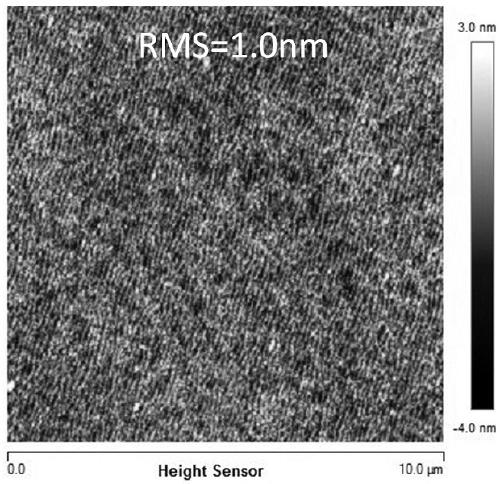
A technology of multiple quantum wells and interface quality, applied in electrical components, circuits, semiconductor devices, etc., can solve the problems of reduced quantum efficiency, large surface undulations, blurred interfaces, etc., and achieves low defect density, smooth surface, and reduced heating effects.

Active Publication Date: 2020-05-22
NO 55 INST CHINA ELECTRONIC SCI & TECHNOLOGYGROUP CO LTD
View PDF5 Cites 0 Cited by
  • Summary
  • Abstract
  • Description
  • Claims
  • Application Information

AI Technical Summary

Problems solved by technology

However, due to the large difference in epitaxial growth conditions between AlGaN and AlN materials, the growth temperature of AlN requires a higher growth temperature, and low-temperature AlN tends to show an island-like growth mode, resulting in problems such as large surface fluctuations and blurred interfaces; while the growth temperature of AlGaN materials is higher than that of AlN Low, too high temperature will cause the decomposition of AlGaN material, resulting in surface roughening, and the formation of non-radiative recombination centers such as vacancy defects and dislocation pits on the surface, resulting in a decrease in quantum efficiency

Method used


Image

  • Growth method for improving interface quality of AlGaN/AlN multi-quantum well
  • Growth method for improving interface quality of AlGaN/AlN multi-quantum well
  • Growth method for improving interface quality of AlGaN/AlN multi-quantum well

Examples


Embodiment 1

[0025] The present invention provides a growth method for improving the interface quality of AlGaN / AlN multiple quantum wells, comprising the following steps:

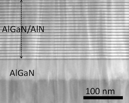
[0026] 1) Select a (0001) surface sapphire substrate, transfer it into the MOCVD system, and grow the nucleation layer, buffer layer, and n-type doped layer in sequence. The nucleation layer is an AlN film with a thickness of 20nm; the buffer layer is an AlN film with a thickness of 1000nm; the n-type doped layer is an AlGaN film with an aluminum composition of 0.6, a thickness of 2500nm, and a doping concentration of 2E19cm 3 .

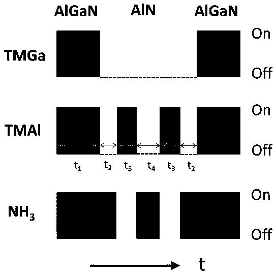
[0027] 2) Carry out the growth of the quantum barrier. The quantum barrier is an AlN layer, the source of group III is TMAl, and the source of group V is high-purity NH 3 , TMAl, NH 3 Alternately feed into the reaction chamber, 4 alternate cycles, TMAl feed time is 6s, NH 3 The penetration time is 6s, the V / III ratio (the molar ratio of the III source to the V source) is 500, the growth t...

Embodiment 2

[0035] The present invention provides a growth method for improving the interface quality of AlGaN / AlN multiple quantum wells, comprising the following steps:

[0036] 1) Select a (0001) surface sapphire substrate, transfer it into the MOCVD system, and grow the nucleation layer, buffer layer, and n-type doped layer in sequence. The nucleation layer is an AlN film with a thickness of 100nm; the buffer layer is an AlGaN film with an aluminum composition of 0.5 and a thickness of 2500nm; the n-type doped layer is an AlGaN film with an aluminum composition of 0.4 and a thickness of 1000nm with a doping concentration of 5E17cm 3 .

[0037] 2) Carry out the growth of the quantum barrier. The quantum barrier is an AlN layer, the source of group III is TMAl, and the source of group V is high-purity NH 3 , TMAl, NH 3 Alternately feed into the reaction chamber, 20 alternate cycles, TMAl feed time is 2s, NH 3 The penetration time is 2s, the V / III ratio (the molar ratio of the III sour...

Embodiment 3

[0045] The present invention provides a growth method for improving the interface quality of AlGaN / AlN multiple quantum wells, comprising the following steps:

[0046] 1) Select a (0001) surface sapphire substrate, transfer it into the MOCVD system, and grow the nucleation layer, buffer layer, and n-type doped layer in sequence. The nucleation layer is an AlN film with a thickness of 50nm; the buffer layer is an AlN film with a thickness of 1500nm; the n-type doped layer is an AlGaN film with an aluminum composition of 0.4, a thickness of 2500nm, and a doping concentration of 1E19cm 3 .

[0047] 2) Carry out the growth of the quantum barrier. The quantum barrier is an AlN layer, the source of group III is TMAl, and the source of group V is high-purity NH 3 , TMAl, NH 3 Alternately feed into the reaction chamber, 2 alternate cycles, TMAl feed time is 6s, NH 3 The penetration time is 6s, the V / III ratio (the molar ratio of the III source to the V source) is 500, the growth t...


PUM

PropertyMeasurementUnit
thicknessaaaaaaaaaa
thicknessaaaaaaaaaa
thicknessaaaaaaaaaa

Abstract

The invention relates to a growth method for improving the interface quality of an AlGaN/AlN multi-quantum well, which is carried out in MOCVD equipment, and is used for interrupting the growth and inhibiting the formation of an interface component gradient layer when an AlGaN quantum well and an AlN quantum barrier are periodically switched; and meanwhile, III-group and V-group sources are periodically and alternately provided in the AlN growth process, so that the pre-reaction between reaction sources is reduced, the transverse migration capability of metal atoms is improved, the AlN surfaceappearance is improved, the interface steepness is enhanced, and the interface quality between AlGaN and AlN is improved. The method has the advantages that the AlN growth temperature can be reduced,the surface smoothness of the AlN is ensured, the method realizes the same temperature growth of AlGaN and AlN, inhibits the formation of an interface component gradient layer, enhances the steepnessof the interface, improves the quality of the interface, is economical, simple and feasible, has good epitaxial material performance, and is an effective solution for realizing the high-quality and low-cost growth of the AlGaN/AlN multi-quantum well structure.

Description

technical field [0001] The invention relates to a growth method for improving the interface quality of AlGaN / AlN multi-quantum wells, and belongs to the technical field of semiconductors. Background technique [0002] The AlGaN semiconductor material has a wide direct bandgap, and the forbidden band width is continuously adjustable from 3.4-6.2eV, so that the corresponding band of its spectrum covers the near-ultraviolet to deep-ultraviolet band (200-365nm). In addition, AlGaN material also has the characteristics of high thermal conductivity, high electron saturation rate, strong breakdown field and good thermal stability, so it is very useful in the preparation of optoelectronic devices such as ultraviolet light-emitting diodes (LEDs), ultraviolet laser diodes, and ultraviolet detectors. attention. Compared with the traditional ultraviolet mercury lamp, the ultraviolet LED light source has the advantages of energy saving, electricity saving, mercury-free, small beam angle...

Claims


Application Information

Patent Timeline
Patent Type & Authority Applications(China)
IPC IPC(8): H01L33/00H01L33/06H01L33/32
CPCH01L33/0025H01L33/0075H01L33/06H01L33/32
Inventor 罗伟科李忠辉
Owner NO 55 INST CHINA ELECTRONIC SCI & TECHNOLOGYGROUP CO LTD
Why Eureka
Try Eureka