Ultraviolet LED chip and manufacturing method thereof

A technology of LED chip and manufacturing method, applied in ion implantation plating, coating, electrical components and other directions, can solve problems such as affecting the light output efficiency of ultraviolet LED chips, and achieve the improvement of current expansion capability, reliability, and voltage reduction. Effect

Pending Publication Date: 2020-05-22
FOSHAN NATIONSTAR SEMICON
View PDF0 Cites 2 Cited by
  • Summary
  • Abstract
  • Description
  • Claims
  • Application Information

AI Technical Summary

Problems solved by technology

However, the materials used in the existing LED manufacturing process have a strong absorption of ultraviolet light, which seriously affects the light extraction efficiency of ultraviolet LED chips.

Method used


Image

  • Ultraviolet LED chip and manufacturing method thereof
  • Ultraviolet LED chip and manufacturing method thereof

Examples


Embodiment 1

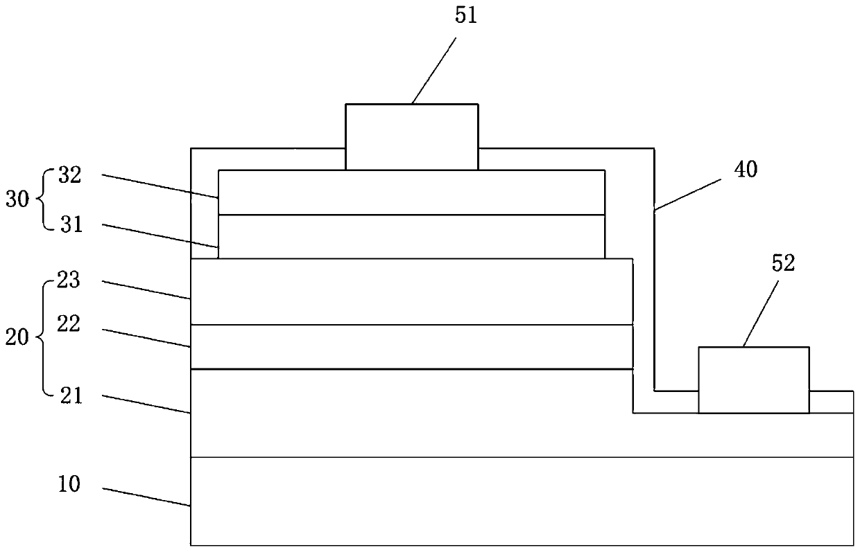
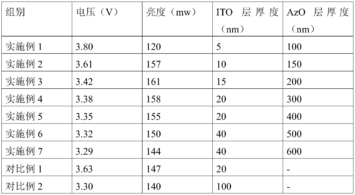
[0062] An ultraviolet LED chip comprises a substrate, an epitaxial layer arranged on the substrate, a transparent conductive layer and an electrode structure arranged on the epitaxial layer, and a protective layer covering the transparent conductive layer and the epitaxial layer.

[0063] The transparent conductive layer includes an ITO layer and an AzO layer, the ITO layer is arranged between the second semiconductor layer and the AzO layer, the thickness of the ITO layer is 5nm, the thickness of the AzO layer is 100nm, and the protective layer Made of boron nitride, 20nm thick.

Embodiment 2

[0065] An ultraviolet LED chip comprises a substrate, an epitaxial layer arranged on the substrate, a transparent conductive layer and an electrode structure arranged on the epitaxial layer, and a protective layer covering the transparent conductive layer and the epitaxial layer.

[0066] The transparent conductive layer includes an ITO layer and an AzO layer, the ITO layer is arranged between the second semiconductor layer and the AzO layer, the thickness of the ITO layer is 10nm, the thickness of the AzO layer is 150nm, and the protective layer Made of boron nitride, 50nm thick.

Embodiment 3

[0068] An ultraviolet LED chip comprises a substrate, an epitaxial layer arranged on the substrate, a transparent conductive layer and an electrode structure arranged on the epitaxial layer, and a protective layer covering the transparent conductive layer and the epitaxial layer.

[0069] The transparent conductive layer comprises an ITO layer and an AzO layer, the ITO layer is arranged between the second semiconductor layer and the AzO layer, the thickness of the ITO layer is 15nm, the thickness of the AzO layer is 200nm, and the protective layer Made of boron nitride, 50nm thick.


PUM

PropertyMeasurementUnit
thicknessaaaaaaaaaa
thicknessaaaaaaaaaa
thicknessaaaaaaaaaa

Abstract

The invention discloses an ultraviolet LED chip and a manufacturing method thereof. The chip comprises a substrate, an epitaxial layer arranged on the substrate, a transparent conductive layer and anelectrode structure which are arranged on the epitaxial layer, and a protective layer covering the transparent conductive layer and the epitaxial layer. The LED chip is characterized in that the transparent conductive layer comprises an ITO layer and an AzO layer, the ITO layer is arranged between the epitaxial layer and the AzO layer, the thickness of the ITO layer is 5-20 nm, and the thickness of the AzO layer is 150-500 nm. According to the transparent conductive layer, through mutual cooperation of the ITO layer and the AzO layer, the light emitting efficiency of the chip is effectively improved, and the voltage is effectively reduced.

Description

technical field [0001] The invention relates to the technical field of light emitting diodes, in particular to an ultraviolet LED chip and a manufacturing method thereof. Background technique [0002] Light-emitting diode, the abbreviation of the English word LED, the main meaning: LED=Light Emitting Diode, is a solid-state semiconductor device that can convert electrical energy into visible light. As a lighting device, compared with traditional lighting devices, light-emitting diodes have considerable advantages—— Long life, high light efficiency, no radiation, low power consumption, green and environmental protection. At present, LEDs are mainly used in fields such as display screens, indicator lights, and backlight sources. [0003] In order to reduce the pollution of blue light, the application of purple light is an important part of healthy lighting. However, the materials used in the existing LED manufacturing process have a strong absorption of ultraviolet light, wh...

Claims


Application Information

Patent Timeline
Patent Type & Authority Applications(China)
IPC IPC(8): H01L33/42C23C14/08C23C14/30
CPCC23C14/08C23C14/30H01L33/42H01L2933/0016
Inventor 仇美懿庄家铭
Owner FOSHAN NATIONSTAR SEMICON
Why Eureka
Try Eureka