Quantum wire laser and preparation method thereof

A laser and quantum wire technology, applied in the field of lasers, can solve the problem of inability to achieve simultaneous lasing of multiple wavelengths, and achieve the effect of easy operation and implementation, and the method is simple and easy to implement.

Inactive Publication Date: 2020-06-12
SHENZHEN INSTITUTE OF INFORMATION TECHNOLOGY
View PDF5 Cites 0 Cited by
  • Summary
  • Abstract
  • Description
  • Claims
  • Application Information

AI Technical Summary

Problems solved by technology

[0004] The purpose of the present invention is to provide a quantum wire laser and its preparation method, aiming to solve the problem that the existing InAs / InP quantum wire laser cannot realize simultaneous lasing of multiple wavelengths

Method used


Image

  • Quantum wire laser and preparation method thereof
  • Quantum wire laser and preparation method thereof
  • Quantum wire laser and preparation method thereof

Examples


preparation example Construction

[0068] An embodiment of the present invention provides a method for preparing a quantum wire laser, including the following steps:

[0069] S1. Select a substrate;

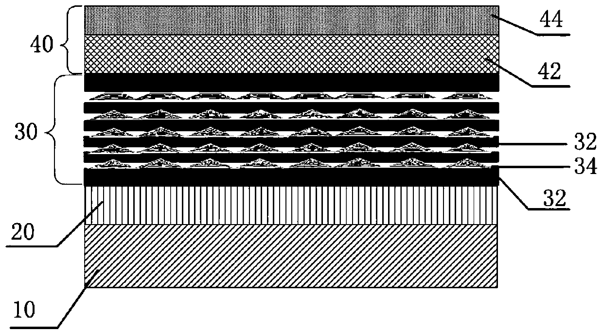
[0070] S2, sequentially growing a buffer layer, an active region, and a top electrode on the substrate;

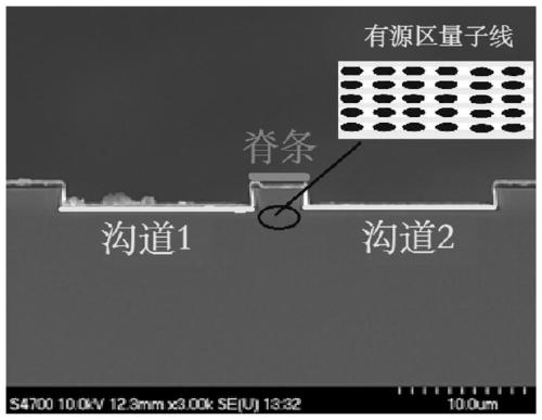
[0071] After etching, a quantum wire laser is obtained;

[0072] Wherein, the active region is obtained by taking the spacer layer as the bottom layer and the top layer by alternately growing the spacer layer and the indium arsenide quantum wire layer.

[0073] In the present invention, a buffer layer, an active region and a top electrode are sequentially grown on a substrate by gas source molecular beam epitaxy (GSMBE), and at least one indium arsenide quantum wire layer is arranged in the active region, and the method is simple and convenient. Advantages of operational implementation.

Embodiment

[0093] (1) By gas source molecular beam epitaxy (GSMBE), a 600nm thick n-InGaAsP buffer layer is first grown on an N-type InP substrate, the doping element is Si, and the doping concentration is 3×10 18 / cm 3 , the growth temperature is 530°C;

[0094] (2) On the n-InGaAsP buffer layer, continue to grow a non-doped InGaAsP lower surface optical waveguide dielectric layer with a thickness of 200nm, the growth temperature is 530°C, and the optical waveguide band gap is 1.05ev (equivalent to a wavelength of 1.18μm);

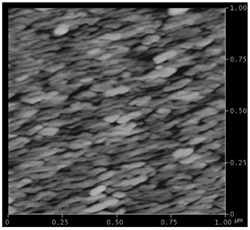
[0095] (3) The quantum wires in the active region are composed of 5 layers of InAs. The growth temperature of each layer of InAs quantum wires is 485°C, the growth rate is 0.1ML / s, the growth thickness is 3.5ML, and the growth time is 35s. AsH 3 The air pressure in the chamber is 630Torr, and the air pressure in the growth chamber is 1.5×10 -5 Torr;

[0096] (4) In order to prevent the interference between each layer of quantum wires, each layer of InAs quantum w...


PUM

PropertyMeasurementUnit
thicknessaaaaaaaaaa
thicknessaaaaaaaaaa
thicknessaaaaaaaaaa

Abstract

The invention belongs to the technical field of lasers, and particularly relates to a quantum wire laser and a preparation method thereof. The quantum wire laser comprises a substrate, a buffer layerarranged on the substrate, an active region arranged on the buffer layer and a top electrode arranged on the active region, wherein the active region comprises N+1 spacer layers and N indium arsenidequantum wire layers, and the spacer layers and the indium arsenide quantum wire layers are alternately arranged; wherein N is an integer greater than or equal to 1. According to the invention, the indium arsenide quantum lines arranged in the active region are non-uniform in size distribution; according to the quantum wire laser, the excitation state of the indium arsenide quantum wire with a larger size is overlapped with the ground state of the indium arsenide quantum wire with a smaller size, so that the obtained quantum wire laser has a very wide gain spectrum, and the effect of simultaneous lasing of multiple wavelengths can be realized under the drive of current injection.

Description

technical field [0001] The invention belongs to the technical field of lasers, and in particular relates to a quantum wire laser and a preparation method thereof. Background technique [0002] The operating wavelength of a semiconductor optoelectronic device is closely related to the semiconductor material used to make the device. With the development of optoelectronic devices, in the pursuit of newer, smaller, and better performance quantum devices, it is found that it is not enough to confine carriers in only one dimension, and it is necessary to confine carriers in two or three dimensions. Fluids achieve quantum confinement, thus forming one-dimensional quantum wires or quantum dots. [0003] Quantum wire / quantum dot lasers have the advantages of high gain, low threshold current, high differential gain and modulation frequency, and their spectral line width has also been significantly improved. After being developed, they have been widely optimized and applied. However,...

Claims


Application Information

Patent Timeline
Patent Type & Authority Applications(China)
IPC IPC(8): H01S5/34H01S5/343
CPCH01S5/341H01S5/34313
Inventor 李世国周志文谭晓玲陈艳张卫丰
Owner SHENZHEN INSTITUTE OF INFORMATION TECHNOLOGY
Why Eureka
Try Eureka