
Vacuum channel type photocathode and preparation method thereof

A photocathode and channel technology, applied in the manufacture of light-emitting cathodes, photoemission cathodes, main electrodes of discharge tubes, etc., can solve the problems of poor stability, short life, low emission current density, etc., to reduce lattice mismatch, The effect of increasing the frequency and increasing the current emission intensity

Pending Publication Date: 2020-07-03
NO 12 RES INST OF CETC
View PDF9 Cites 0 Cited by
  • Summary
  • Abstract
  • Description
  • Claims
  • Application Information

AI Technical Summary

Problems solved by technology

[0006] The purpose of the present invention is to provide a vacuum channel photocathode with high current density and high stability and a method for preparing the photocathode in view of the current situation of low emission current density, short life and poor stability of the existing photocathode.

Method used


Image

  • Vacuum channel type photocathode and preparation method thereof
  • Vacuum channel type photocathode and preparation method thereof
  • Vacuum channel type photocathode and preparation method thereof

Examples


preparation example Construction

[0042] The present invention further provides a method for preparing a photocathode, comprising the following steps:

[0043] Use organic solvents, deionized water, acidic or alkaline solutions, etc. to clean the pollutants on the surface of the cathode substrate material;

[0044] Using epitaxial techniques such as MOCVD or MBE to grow a buffer layer on the surface of the cathode substrate material;

[0045] Using techniques such as MOCVD or MBE to alternately grow the first semiconductor material and the second semiconductor material on the buffer layer to obtain a periodic structure, and further form a surface semiconductor layer on the periodic structure to obtain a cathode emission layer;

[0046] Fabricate a vacuum channel structure on the surface of the obtained cathode emission layer using micro-nano processing technology or ion beam focused etching technology, wherein the area of ​​the vacuum channel on the side close to the substrate is smaller than the area of ​​the...

Embodiment 1

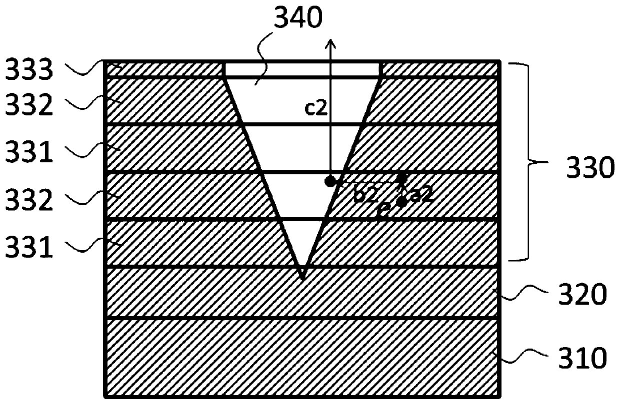
[0051] Combine below figure 2 Specifically illustrate a schematic diagram of a vacuum channel photocathode according to Embodiment 1 of the present invention, the photocathode includes a sapphire substrate, and has a GaN layer as the first semiconductor material layer, and an Al layer as the second semiconductor layer. 0.3 Ga 0.7 A cathode emitter layer with a periodic structure of N layers and an inverted conical vacuum channel.

[0052] Specifically, the vacuum channel photocathode includes a sapphire substrate 310 on which Al 0.3 Ga 0.7 The N layer is used as a buffer layer 320 , and a cathode emission layer 330 is formed on the buffer layer, including a periodic structure of alternately arranged first semiconductor materials 331 and second semiconductor materials 332 and a surface semiconductor layer 333 . The thickness of the first semiconductor layer GaN layer is 35nm, the second semiconductor layer Al 0.3 Ga 0.7 The thickness of the N layer is 65 nm, the first sem...

Embodiment 2

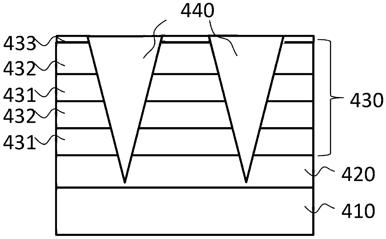
[0061] image 3 According to the strip-shaped vacuum channel type photocathode according to the embodiment 2 of the present invention, the photocathode comprises a GaAs substrate, and has a GaAs layer as a first semiconductor layer, a second semiconductor layer Al 0.55 Ga 0.45 Cathode emitter layer with periodic structure of As layer and two vacuum channels.

[0062] Specifically, the vacuum channel photocathode includes a GaAs substrate layer 410, an Al 0.55 Ga 0.45 As buffer layer 420, a cathode emission layer 430 formed on the buffer layer, including alternately arranged first semiconductor material layers GaAs layers 431 and second semiconductor material layers Al 0.55 Ga 0.45 As layer 432, each Al 0.55 Ga 0.45 The thicknesses of the As layer and the GaAs layer are 50nm and 60nm respectively, the cycle number T of the two crystals is 8; the thickness of the surface GaAs layer 433 is 50nm. The vacuum channel structure is a strip structure, the width of the vacuum cha...


PUM

PropertyMeasurementUnit
thicknessaaaaaaaaaa
thicknessaaaaaaaaaa
thicknessaaaaaaaaaa

Abstract

The invention discloses a vacuum channel type photocathode and a preparation method thereof. The vacuum channel type photocathode comprises a substrate and a cathode emission layer formed on the substrate, wherein the cathode emission layer comprises first semiconductor material layers and second semiconductor material layers which are periodically and alternately arranged, and a channel formed inthe cathode emission layer, and the area of the side, close to the substrate, of the channel is smaller than that of the surface of the cathode emission layer. The photocathode provided by the invention can generate high emission current density and effectively shorten the response time of the cathode, so that the photocathode has the capability of emitting terahertz frequency electronic pulses,and can be applied to optical modulation vacuum microwave devices, free electron lasers, light sources and the like.

Description

technical field [0001] The invention relates to the field of electric vacuum components. More specifically, it relates to a vacuum channel photocathode, an electron source including the photocathode, and a method for preparing the photocathode. Background technique [0002] The amplification, switching and modulation of electrical signals in the early days of electronics research were all based on vacuum tubes. With the development of information technology, vacuum tubes gradually developed into magnetrons, klystrons, traveling wave tubes, gyrotrons, etc., and their operating frequencies also From low frequency to terahertz frequency, it is the core component of radio communication. The working principle of a vacuum device is to achieve signal amplification, switching and modulation by changing the state of electron movement, and the cathode as an electron emission component becomes the key to determine the performance of a vacuum device. [0003] Traditional vacuum device...

Claims


Application Information

Patent Timeline
Patent Type & Authority Applications(China)
IPC IPC(8): H01J1/34H01J9/12
CPCH01J9/12H01J1/34
Inventor 郝广辉邵文生张珂
Owner NO 12 RES INST OF CETC
Learn More