Microwave-assisted atomic layer deposition method and reactor

An atomic layer deposition, microwave-assisted technology, applied in coating, metal material coating process, gaseous chemical plating, etc., can solve the problems of high resistivity of the barrier layer, high impurity content, difficult to conduct barrier layers, etc.

Active Publication Date: 2020-07-07
FUDAN UNIV +1
View PDF3 Cites 2 Cited by
  • Summary
  • Abstract
  • Description
  • Claims
  • Application Information

AI Technical Summary

Problems solved by technology

However, because the metal precursors and reactants used in the atomic layer deposition process are difficult to fully react, resulting in high impurity content, resulting in generally high resistivity of the barrier layer, it is difficult to serve as a good conductive barrier layer

Method used


Image

  • Microwave-assisted atomic layer deposition method and reactor
  • Microwave-assisted atomic layer deposition method and reactor
  • Microwave-assisted atomic layer deposition method and reactor

Examples


Embodiment Construction

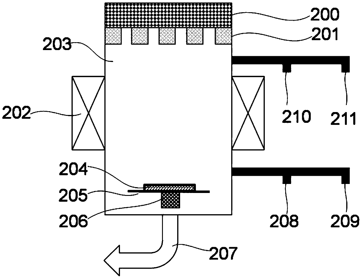
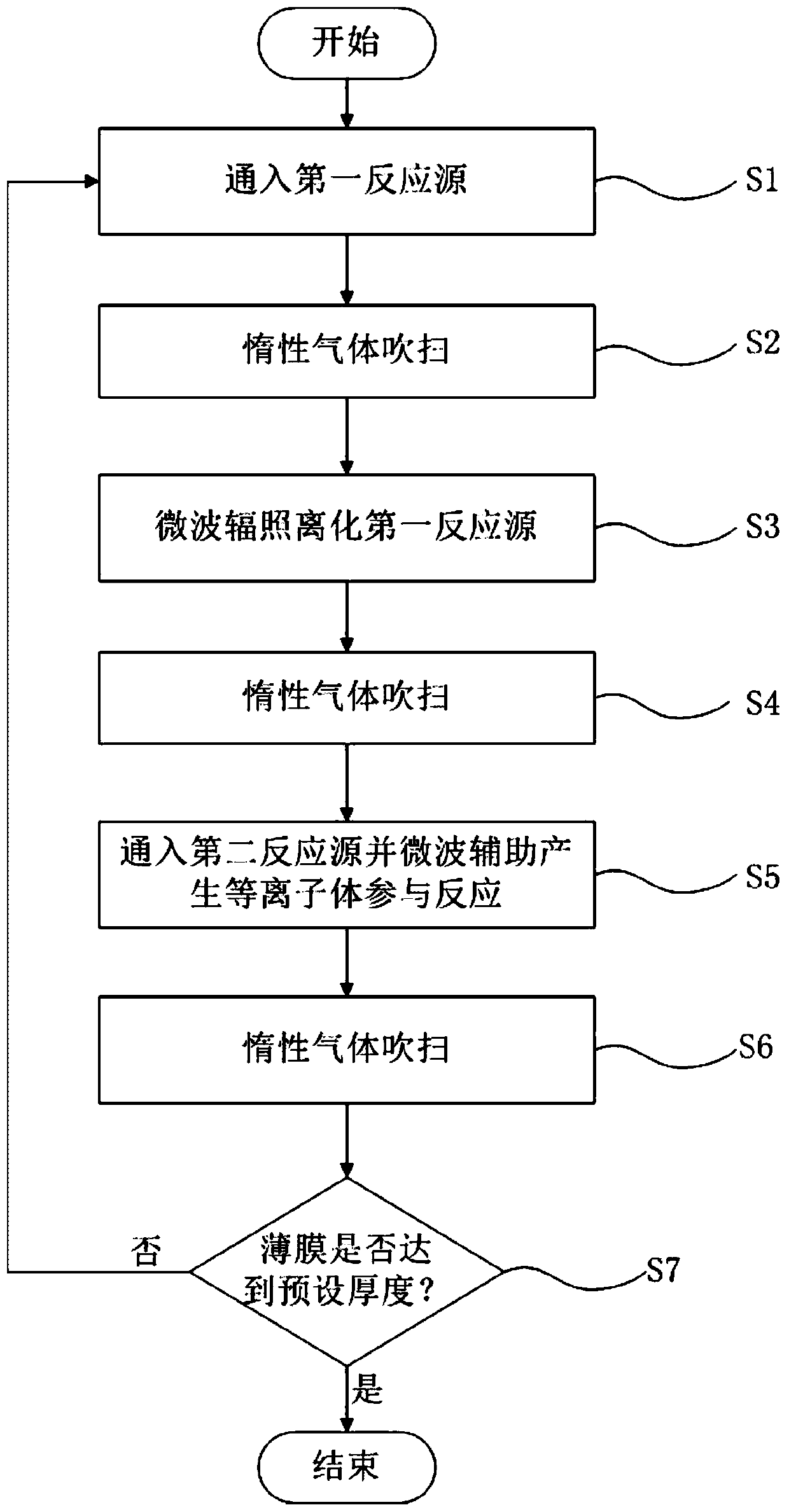
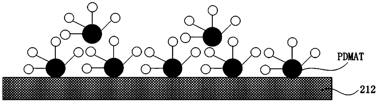
[0036] The present invention will be further introduced below in conjunction with the embodiments and accompanying drawings. It should be understood that the examples are only used to explain the present invention, not to limit the present invention. All other embodiments obtained by persons of ordinary skill in the art without creative efforts fall within the protection scope of the present invention.

[0037] In the description of the present invention, it should be noted that the orientation or positional relationship indicated by the terms "upper", "lower", "vertical" and "horizontal" are based on the orientation or positional relationship shown in the drawings, and are only for convenience The present invention is described and simplified descriptions do not indicate or imply that the device or element referred to must have a specific orientation, be constructed and operate in a specific orientation, and thus should not be construed as limiting the present invention. In ...


PUM


Abstract

The invention belongs to the technical field of integrated circuit manufacturing, and particularly relates to a microwave-assisted atomic layer deposition method and reactor. The atomic layer deposition reactor comprises a reaction chamber, a microwave source, a vacuum pump and gas pipelines, wherein the top of the reaction chamber is provided with a quartz window, a substrate tray is arranged inside the reaction chamber, the side wall of the reaction chamber is provided with a magnet exciting coil, the microwave source is arranged above the quartz window, the vacuum pump is used for adjustingthe vacuum degree of the reaction chamber, the gas pipelines comprise a first reaction source gas conveying pipeline, a second reaction source gas conveying pipeline and an inert gas pipeline which are used for conveying a first reaction source, a second reaction source and inert gas respectively, the microwave source carries out microwave irradiation decomposition on the first reaction source, the microwave source and the magnet exciting coil jointly generate a microwave electron cyclotron resonance source, and the second reaction source is excited to form high-energy plasmas. According to the microwave-assisted atomic layer deposition method and reactor, the conductivity and ductility of a thin film can be effectively improved, an ideal step coverage rate and the accurate thin film thickness control capability are achieved, and the requirements of an advanced CMOS integrated circuit process can be met.

Description

technical field [0001] The invention belongs to the technical field of integrated circuit manufacturing, and in particular relates to a microwave-assisted atomic layer deposition method and a reactor. Background technique [0002] For the back-end process of copper interconnection, metal nitrides such as tantalum nitride and titanium nitride need to be filled in deep trenches and vias as copper diffusion barrier layers. As the process node continues to advance, the aspect ratio of the via hole continues to increase, resulting in poor step coverage and partial blockage in the traditional physical vapor deposition (PVD) process when filling the barrier layer. In order to solve this problem, the atomic layer deposition process was introduced as a barrier filling method, because the atomic layer deposition process has the characteristics of self-limited growth, and the grown film has good conformality and high step coverage. However, because the metal precursors and reactants u...

Claims


Application Information

Patent Timeline
Patent Type & Authority Applications(China)
IPC IPC(8): C23C16/455C23C16/34
CPCC23C16/34C23C16/45536C23C16/45544
Inventor 朱宝陈琳孙清清张卫
Owner FUDAN UNIV
Why Eureka
Try Eureka