A polishing method for a thin-film lithium niobate optical waveguide chip polishing device

A polishing device and lithium niobate technology, which is applied in the field of integrated optical chip manufacturing and micro-nano processing, can solve the problems of large roughness, high price, and damage to the optical waveguide side wall and surface, and achieve the etching surface and waveguide. The side wall is smooth, the process equipment is simple, and the effect of surface damage is small

Active Publication Date: 2022-04-29
NO 55 INST CHINA ELECTRONIC SCI & TECHNOLOGYGROUP CO LTD
View PDF6 Cites 0 Cited by
  • Summary
  • Abstract
  • Description
  • Claims
  • Application Information

AI Technical Summary

Problems solved by technology

[0002] Optical waveguide is the basic unit for building integrated optical functional devices and chips. Its transmission loss mainly depends on the scattering loss caused by the roughness of the side wall and surface of the optical waveguide, and the roughness of the surface and side wall of the optical waveguide depends on the etching of the optical waveguide. Technology, especially for thin-film lithium niobate crystal materials, its processing technology is more difficult than silicon oxide, silicon and polymer materials. At present, the etching of thin-film lithium niobate optical waveguide mainly adopts argon ion dry etching. The principle is to use Argon ions bombard the surface of the thin-film lithium niobate material. After dry etching, the sidewall and surface roughness of the optical waveguide are usually large, and the etching products generated during the etching process will continue to accumulate on the optical waveguide. The sidewall and surface further deteriorate the surface roughness of the optical waveguide, resulting in higher optical waveguide transmission loss
[0003] At present, there are two main methods to reduce the surface roughness of thin-film lithium niobate optical waveguide: one is to use inductively coupled plasma dry etching, and to reduce the deposition of etching products by continuously optimizing the radio frequency power and etching pressure. The method has high requirements on the performance of the etching equipment, is expensive, and has a limited effect on reducing the roughness of the etching surface; the second is to use polishing technology to smooth the surface of the optical waveguide, which is mainly used in micro-nano processing technology. Polishing on the plane of the wafer substrate, the method is to fix the wafer substrate on the polishing fixture, place the plane to be polished upside down on the polishing pad of the polishing machine, and use the polishing liquid to physically rub and chemically corrode the plane to achieve Polishing of the substrate plane, however, for the etched optical waveguide, due to the existence of the optical waveguide pattern, the traditional polishing process is difficult to polish the side wall of the optical waveguide, and the polishing process will cause damage to the surface of the optical waveguide

Method used


Image

  • A polishing method for a thin-film lithium niobate optical waveguide chip polishing device
  • A polishing method for a thin-film lithium niobate optical waveguide chip polishing device
  • A polishing method for a thin-film lithium niobate optical waveguide chip polishing device

Examples


Embodiment 1

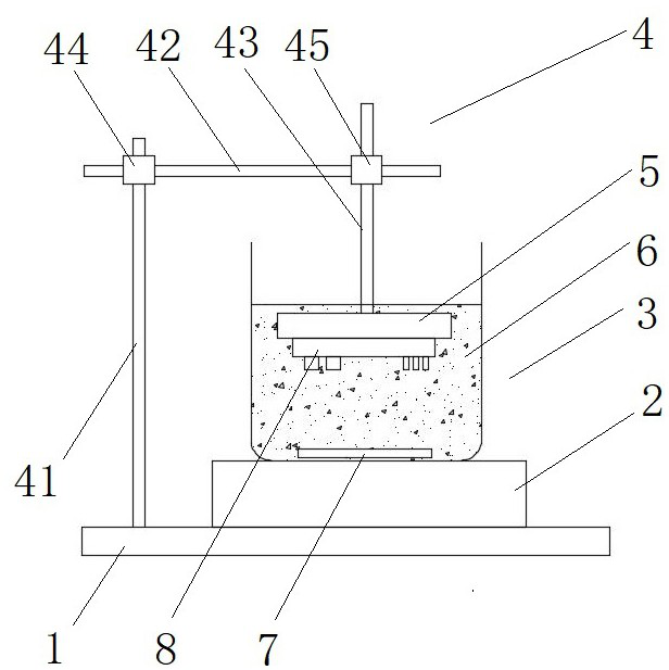
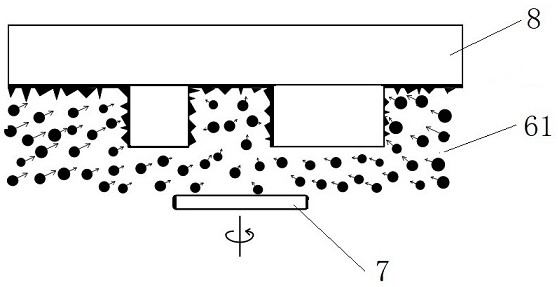
[0035]Add a rough polishing solution 61 with a diameter of 100 nm of silicon oxide polishing particles in the polishing container 3, then install the thin-film lithium niobate optical waveguide chip 8 to be polished on the chip holder 5, and immerse it in the rough polishing solution 61, and start magnetic stirring Stage 2, drives the magnetic rotor 7 to rotate at a high speed to stir the rough polishing solution 61, so that the rough polishing solution 61 flows into contact with the surface of the lithium niobate chip 8 to be polished, and the rough polishing particles in the rough polishing solution 61 and the niobate thin film to be polished The surface of the lithium optical waveguide chip 8 is in semi-contact and sliding contact, and the alkaline ions in the polishing solvent of the rough polishing solution 61 react chemically with the surface of the thin-film lithium niobate optical waveguide chip 8 to be polished. Chemical etching and flow erosion along the direction par...

Embodiment 2

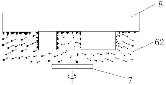
[0038] Add a rough polishing solution 61 with a diameter of silicon oxide polishing particles of 650 nm in the polishing container 3, then install the thin-film lithium niobate optical waveguide chip 8 to be polished on the chip holder 5, and immerse it in the rough polishing solution 61, and start magnetic stirring Stage 2, drives the magnetic rotor 7 to rotate at a high speed to stir the rough polishing solution 61, so that the rough polishing solution 61 flows into contact with the surface of the lithium niobate chip 8 to be polished, and the rough polishing particles in the rough polishing solution 61 and the niobate thin film to be polished The surface of the lithium optical waveguide chip 8 is in semi-contact and sliding contact, and the alkaline ions in the polishing solvent of the rough polishing solution 61 react chemically with the surface of the thin-film lithium niobate optical waveguide chip 8 to be polished. Chemical etching and flow erosion along the direction pa...

Embodiment 3

[0041] Add a rough polishing solution 61 with a diameter of silicon oxide polishing particles of 850 nm in the polishing container 3, then install the thin-film lithium niobate optical waveguide chip 8 to be polished on the chip holder 5, and immerse it in the rough polishing solution 61, and start magnetic stirring Stage 2, drives the magnetic rotor 7 to rotate at a high speed to stir the rough polishing solution 61, so that the rough polishing solution 61 flows into contact with the surface of the lithium niobate chip 8 to be polished, and the rough polishing particles in the rough polishing solution 61 and the niobate thin film to be polished The surface of the lithium optical waveguide chip 8 is in semi-contact and sliding contact, and the alkaline ions in the polishing solvent of the rough polishing solution 61 react chemically with the surface of the thin-film lithium niobate optical waveguide chip 8 to be polished. Chemical etching and flow erosion along the direction pa...


PUM

PropertyMeasurementUnit
diameteraaaaaaaaaa
diameteraaaaaaaaaa
heightaaaaaaaaaa

Abstract

A thin-film lithium niobate optical waveguide chip polishing device and polishing method proposed by the present invention use a magnetic stirring table to drive a magnetic rotor to rotate in a polishing solution, and then stir the polishing solution to flow into contact with the surface of the chip, and the polishing particles therein are in contact with the dry Semi-contact or sliding contact occurs on the surface of the chip etched by the method, accompanied by a small amount of particle bombardment. At the same time, the alkaline ions in the polishing solvent react chemically with the etched surface. Chemical etching and particle bombardment in the parallel direction of the surface, and then remove the etching products deposited on the dry etching surface and the peaks and protrusions produced by dry etching, so as to achieve the smoothing effect of the etching surface and the side wall of the waveguide. Compared with traditional contact mechanical grinding and polishing and chemical mechanical polishing methods, it has the advantages of simple structure, easy operation, low cost and less surface damage.

Description

technical field [0001] The invention relates to the field of integrated optical chip manufacturing and micro-nano processing, in particular to a polishing method for a thin-film lithium niobate optical waveguide chip polishing device. Background technique [0002] Optical waveguide is the basic unit for building integrated optical functional devices and chips. Its transmission loss mainly depends on the scattering loss caused by the roughness of the side wall and surface of the optical waveguide, and the roughness of the surface and side wall of the optical waveguide depends on the etching of the optical waveguide. Technology, especially for thin-film lithium niobate crystal materials, its processing technology is more difficult than silicon oxide, silicon and polymer materials. At present, the etching of thin-film lithium niobate optical waveguide mainly adopts argon ion dry etching. The principle is to use Argon ions bombard the surface of the thin-film lithium niobate mat...

Claims


Application Information

Patent Timeline
Patent Type & Authority Patents(China)
IPC IPC(8): C25F3/20
CPCC25F3/20
Inventor 唐杰钱广孔月婵陈堂胜
Owner NO 55 INST CHINA ELECTRONIC SCI & TECHNOLOGYGROUP CO LTD
Why Eureka
Try Eureka