An electron beam divergence angle measuring device and its preparation method and measurement method

A measuring device and electron beam technology, applied in measuring devices, radiation measurement, X/γ/cosmic radiation measurement, etc., can solve the extremely high collimation requirements of the experimental device, which is not suitable for the measurement of the divergence angle of the electron beam, and is difficult to measure On-site development and other issues to achieve the effect of easy control, high precision and simple operation

Active Publication Date: 2021-12-28
INST OF ELECTRICAL ENG CHINESE ACAD OF SCI
View PDF12 Cites 0 Cited by
  • Summary
  • Abstract
  • Description
  • Claims
  • Application Information

AI Technical Summary

Problems solved by technology

Conventional methods for measuring the divergence angle of electron beams include fluorescent screen method, multi-slit method, single-slit scanning method and pepper hole method, etc., but these methods have low measurement accuracy.
At present, the more advanced method is the Cherenkov radiation method, such as the literature "Research on advanced measurement methods for high-brightness electron beam emittance, beam length and beam spot (Ph. The distribution measurement device and measurement method (CN106970411A) introduces the Cerenkov radiation method to measure the divergence angle of the electron beam, but this measurement method has extremely high requirements on the collimation of the experimental device, and the system adjustment is complicated, which is not easy to carry out at the measurement site. and other problems, it is not suitable for the measurement of electron beam divergence angle of reflective high energy electron diffractometer

Method used


Image

  • An electron beam divergence angle measuring device and its preparation method and measurement method
  • An electron beam divergence angle measuring device and its preparation method and measurement method

Examples


Embodiment 1

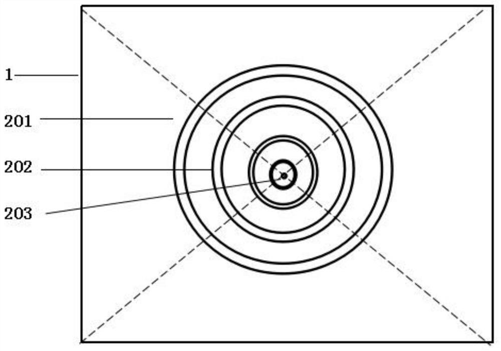
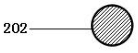
[0026] like Figure 1-2 , The present embodiment provides an electron beam divergence angle measuring means, the measuring device applied to a reflection high energy electron diffraction apparatus comprising a screen and a micro-nano tungsten pattern 201, a conventional phosphor screen the phosphor screen 1, a square shape, while length 20mm ,; thickness of 1mm. Tungsten micro-nano pattern 201 as a plurality of concentric circles, concentric circles of 10 m minimum radius, maximum radius of 150 m, 10 m radius interval, wherein the concentric circles deposited from tungsten hexacarbonyl tungsten wire 202 is formed, the shape of the tungsten wire of 202 cylindrical with a diameter of 50nm.

[0027] Measuring device for preparing reflection high energy electron diffraction divergence angle of the electron beam, comprising the steps of:

[0028] 1, the cleaning surface of the faceplate 1: 1 on the screen inside a helium ion microscope to be vacuum evacuated to 10 -3 When Pa or less, us...

Embodiment 2

[0033] An electron beam measuring device in the present embodiment the divergence angle, such as figure 1 , The phosphor screen including a micro-nano pattern 201 and tungsten. 1 is a conventional phosphor screen the phosphor screen, the shape of a square with a side length of 20-30mm; thickness of 3mm. Tungsten micro-nano pattern 201 are concentric, the minimum radius of 10 m, the maximum radius of 150 m, an interval of 20 m radius, wherein tungsten hexacarbonyl, tungsten deposited from line 202, is cylindrical in shape, having a diameter of 150nm.

[0034] Measuring device for preparing reflection high energy electron diffraction divergence angle of the electron beam, comprising the steps of:

[0035] 1, the cleaning surface of the faceplate 1: 1 on the screen inside a helium ion microscope to be vacuum evacuated to 10 -3 When Pa or less, using ions washed for 5 minutes to remove surface oxides and contaminants a phosphor screen;

[0036] 2, tungsten micro-nano pattern 201 Prepa...

Embodiment 3

[0038] Electron beam divergence angle of the measuring device of the present embodiment, as figure 1 , The phosphor screen including a micro-nano pattern 201 and tungsten. 1 is a conventional phosphor screen the phosphor screen, the shape of a square with a side length of 25mm; thickness of 2mm. Tungsten micro-nano pattern 201 are concentric, the minimum radius of 10 m, the maximum radius of 150 m, 15 m radius interval, wherein tungsten hexacarbonyl, tungsten deposited from line 202, is cylindrical in shape, having a diameter of 100nm.

[0039] Measuring device for preparing reflection high energy electron diffraction divergence angle of the electron beam, comprising the steps of:

[0040] 1, the cleaning surface of the faceplate 1: 1 on the screen inside a helium ion microscope to be vacuum evacuated to 10 -3 When Pa or less, using ions washed four minutes to remove surface oxides and contaminants a phosphor screen;

[0041] 2, tungsten micro-nano pattern 201 Preparation: After th...


PUM

PropertyMeasurementUnit
lengthaaaaaaaaaa
thicknessaaaaaaaaaa
lengthaaaaaaaaaa

Abstract

The invention discloses a device for measuring electron beam divergence angle and its preparation method and measurement method. It comprises a fluorescent screen and a tungsten micro-nano pattern. Tungsten hexacarbonyl is deposited on the fluorescent screen through a helium ion microscope to form the tungsten micro-nano pattern. The tungsten micro-nano pattern is a plurality of concentric circles, and the center of the concentric circles is located at the center of the fluorescent screen. Use helium ion microscope ion-assisted deposition to build tungsten micro-nano patterns on the fluorescent screen. When the fluorescent screen is moved, the shape and size of the spots hit by the electron beam on the fluorescent screen will change. Directly measure the electron beam according to the size and size of the tungsten micro-nano patterns. Beam spot and electron beam divergence angle. The device has the advantages of multi-function, high measurement precision, simple operation and the like; the preparation method has the advantages of high precision, easy control, simple process and the like.

Description

Technical field [0001] Technical Field The present invention relates to an electron beam divergence angle measurements, in particular, it relates to an electron beam divergence angle measuring method and measuring apparatus and its preparation method. Background technique [0002] Reflection high energy electron diffraction (the RHEED) mainly composed of an electron gun and a phosphor screen, is a powerful tool to monitor in situ analysis and surface science today and engineering artificial materials at the atomic level synthesis. In order to improve the resolution of electron diffraction, electron beam divergence angle requirement is relatively high, generally less than 0.1 mrad. Conventional methods for measuring the electron beam divergence angle of the fluorescent screen, multi stitch, single slit scanning method and pepper hole method, but these methods present the measurement accuracy. More advanced method is to Cherenkov radiation, "Study on Measurement Method advanced hig...

Claims


Application Information

Patent Timeline
Patent Type & Authority Patents(China)
IPC IPC(8): G01T1/29G01T7/00
CPCG01T1/2907G01T7/00
Inventor 马玉田刘俊标韩立赵伟霞王鹏飞
Owner INST OF ELECTRICAL ENG CHINESE ACAD OF SCI
Why Eureka
Try Eureka