Semiconductor power device structure and manufacturing method thereof

A technology of power devices and manufacturing methods, applied in semiconductor/solid-state device manufacturing, semiconductor devices, electrical components, etc., to reduce the risk of leakage current, simplify the process flow, and simplify the process steps

Inactive Publication Date: 2020-07-14
捷捷微电(上海)科技有限公司
View PDF5 Cites 3 Cited by
  • Summary
  • Abstract
  • Description
  • Claims
  • Application Information

AI Technical Summary

Problems solved by technology

[0005] The object of the present invention is to provide a new semiconductor power device structure and manufacturing method thereof. There is no overlapping area between the gate polysilicon and the split gate polysilicon of the present invention, so the parasitic capacitance between the source and the gate is extremely small, and It greatly reduces the risk of leakage current between the source and the gate, and solves the problems caused by traditional split-gate MOSFETs. In addition to improving device characteristics, it also improves device reliability.

Method used


Image

  • Semiconductor power device structure and manufacturing method thereof
  • Semiconductor power device structure and manufacturing method thereof
  • Semiconductor power device structure and manufacturing method thereof

Examples


Embodiment Construction

[0056] The following will clearly and completely describe the technical solutions in the embodiments of the present invention with reference to the accompanying drawings in the embodiments of the present invention. Obviously, the described embodiments are only some, not all, embodiments of the present invention. Based on the embodiments of the present invention, all other embodiments obtained by persons of ordinary skill in the art without making creative efforts belong to the protection scope of the present invention.

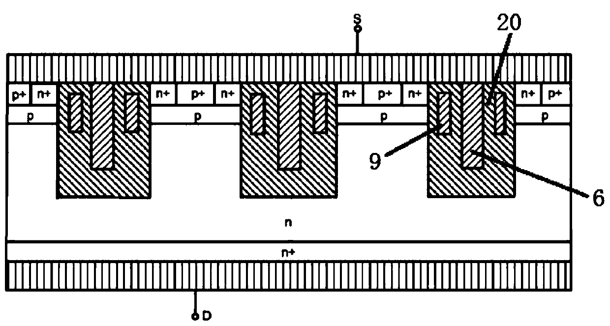
[0057] Figure 3A to Figure 3Q A method for manufacturing a semiconductor power device structure according to an embodiment of the present invention is shown, including the following steps:

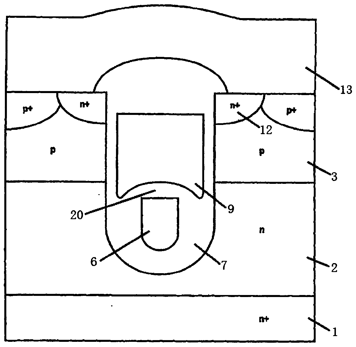
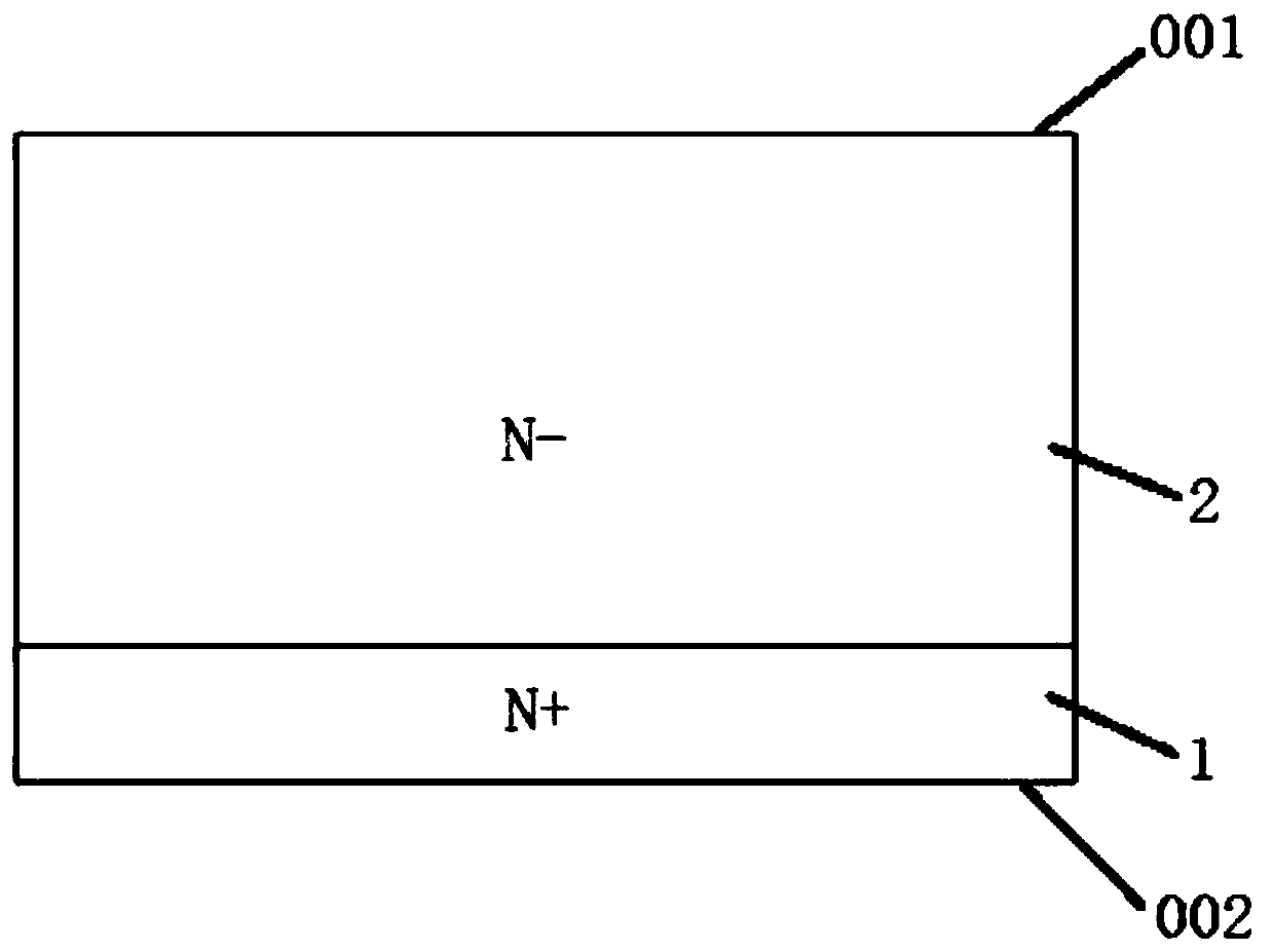
[0058] Step 1, such as Figure 3A As shown, a heavily doped N+ type substrate 1 is selected, and a lightly doped N-type epitaxial layer 2 is formed on the N+ type substrate 1, and the upper surface of the N-type epitaxial layer 2 is the first main surface 001 , and the ...


PUM


Abstract

The invention discloses a semiconductor power device structure and a manufacturing method thereof. The structure comprises a substrate of a first conductivity type and an epitaxial layer of the firstconductivity type on the substrate; a well region of a second conductive type is arranged at the upper part of the epitaxial layer; a control gate trench is arranged between the well regions; a separation gate groove is formed in the bottom of the control gate groove; the separation gate trench is filled with separation gate polycrystalline silicon and a separation gate oxide layer wrapping the side surface and the bottom surface of the separation gate polycrystalline silicon; wherein the separation gate polycrystalline silicon is communicated with the control gate trench, gate oxide layers are arranged on the side wall and the bottom wall of the control gate trench, the gate oxide layers cover the tops of the separation gate oxide layers, and gate polycrystalline silicon is arranged on the side wall of the control gate trench formed by the gate oxide layers; and the inner side of the gate polycrystalline silicon is positioned in a region outside the side wall of the separation gate polycrystalline silicon. No overlapping area exists between the grid polysilicon and the separation grid polysilicon, the parasitic capacitance between the source electrode and the grid electrode is very small, and the risk of current leakage between the source electrode and the grid electrode is greatly reduced.

Description

technical field [0001] The invention relates to the technical field of semiconductors, in particular to a semiconductor power device structure and a manufacturing method thereof. Background technique [0002] Trench power MOSFET is a new high-efficiency switching device developed after planar VDMOS. It is widely used in the field of power electronics because of its high input impedance, small driving current, fast switching speed, and good high-temperature characteristics. High breakdown voltage, high current, and low on-resistance are the most critical indicators of power MOSFETs. The breakdown voltage is related to the value of on-resistance. In the process of MOSFET design, high breakdown voltage and low on-resistance cannot be obtained at the same time. Balance each other between the two. [0003] In order to obtain a higher breakdown voltage and lower on-resistance as possible, a new type of split-gate structure MOSFET device has emerged. Compared with the ordinary tre...

Claims


Application Information

Patent Timeline
Patent Type & Authority Applications(China)
IPC IPC(8): H01L21/336H01L21/28H01L29/423H01L29/78
CPCH01L29/66666H01L21/28008H01L29/4236H01L29/42364H01L29/7828H01L29/7831
Inventor 黄健孙闫涛陈则瑞顾昀浦宋跃桦吴平丽樊君张丽娜
Owner 捷捷微电(上海)科技有限公司
Why Eureka
Try Eureka