Homojunction magnetoresistive device of magnetic two-dimensional semiconductor, preparation method and application thereof

A technology of two-dimensional semiconductor and magnetoresistive devices, which can be used in fields such as magnetic field-controlled resistors, parts of electromagnetic equipment, and manufacturing/processing of electromagnetic devices, which can solve problems such as limited application

Active Publication Date: 2022-03-18
INST OF SEMICONDUCTORS - CHINESE ACAD OF SCI
View PDF5 Cites 0 Cited by
  • Summary
  • Abstract
  • Description
  • Claims
  • Application Information

AI Technical Summary

Problems solved by technology

However, their non-magnetic properties limit their application in the field of magnetic materials.

Method used


Image

  • Homojunction magnetoresistive device of magnetic two-dimensional semiconductor, preparation method and application thereof
  • Homojunction magnetoresistive device of magnetic two-dimensional semiconductor, preparation method and application thereof
  • Homojunction magnetoresistive device of magnetic two-dimensional semiconductor, preparation method and application thereof

Examples


preparation example Construction

[0046] The present invention also discloses a method for preparing the homojunction magnetoresistive device as described above, including:

[0047] Preparing a silicon dioxide layer on a silicon wafer;

[0048] preparing a first nanosheet on the silicon dioxide layer;

[0049] transferring a second nanosheet on the first nanosheet, placing a portion of the second nanosheet on the first nanosheet to form a partial overlap;

[0050] The source and the drain are respectively prepared on the first nanosheet and the second nanosheet, and the source and the drain are respectively located on the first nanosheet and the second nanosheet without intersecting, that is, the homojunction magnetoresistive device is obtained .

[0051] In some embodiments of the present invention, both the first nanosheet and the second nanosheet are Fe x sn 1-x S 2 Nanosheets;

[0052] In some embodiments of the present invention, the Fe x sn1-x S 2 The preparation method of nanosheet comprises: Sn...

Embodiment 1

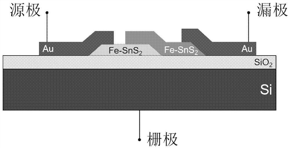
[0080] Such as figure 1 Shown, Si / SiO 2 On the substrate, two layers of Fe 0.021 sn 0.979 S 2 The thin slices are provided with metal electrodes on the two edges of the two thin slices. figure 1 A cross-sectional schematic diagram of the device.

[0081] The lower layer Fe shown in this example 0.021 sn 0.979 S 2 The layer thickness is about 12nm;

[0082] The upper layer Fe shown in this example 0.021 sn 0.979 S 2 The layer thickness is about 25 nm.

[0083] The annealing temperature and time used in this embodiment are annealing at 150° C. for 60 minutes.

[0084] Both the source electrode and the drain electrode are thermally evaporated Au electrodes with a thickness of about 46nm. When testing, use a bonding machine to draw electrodes from the source and drain electrodes and connect them to external circuits.

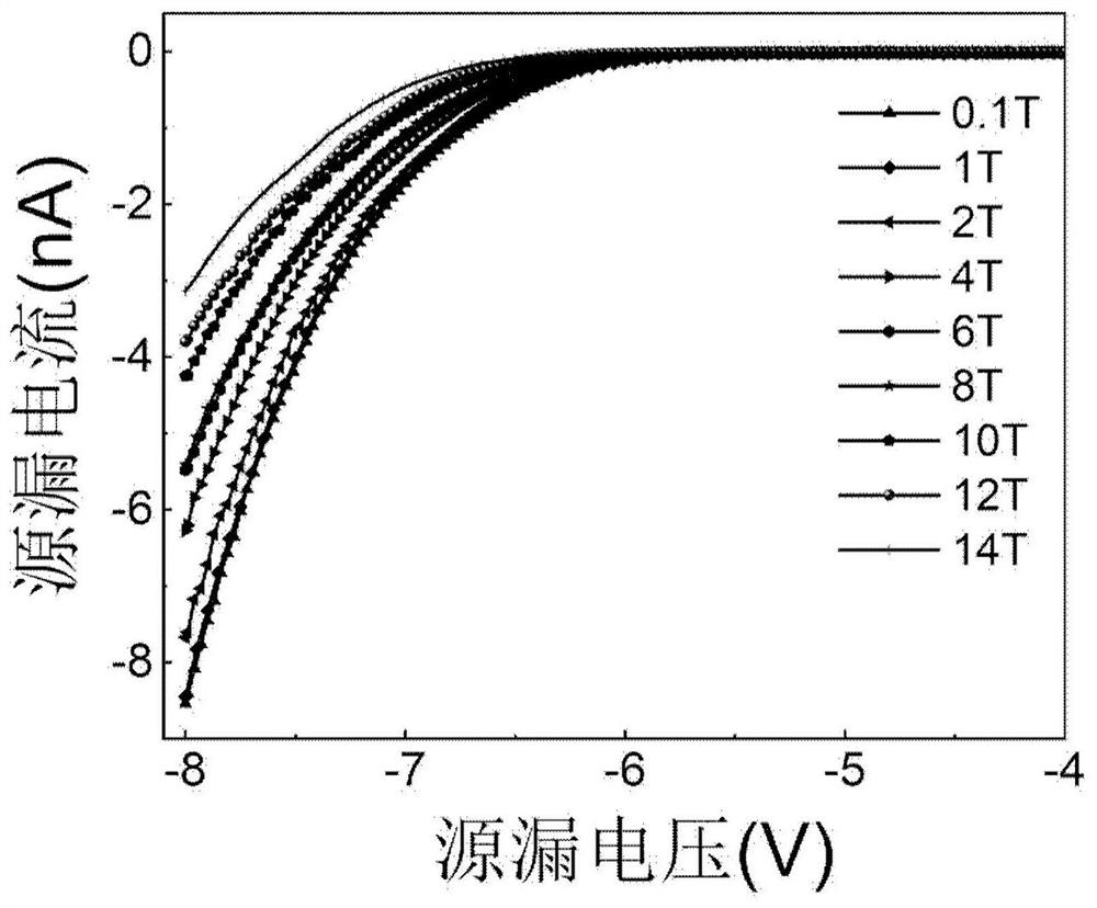
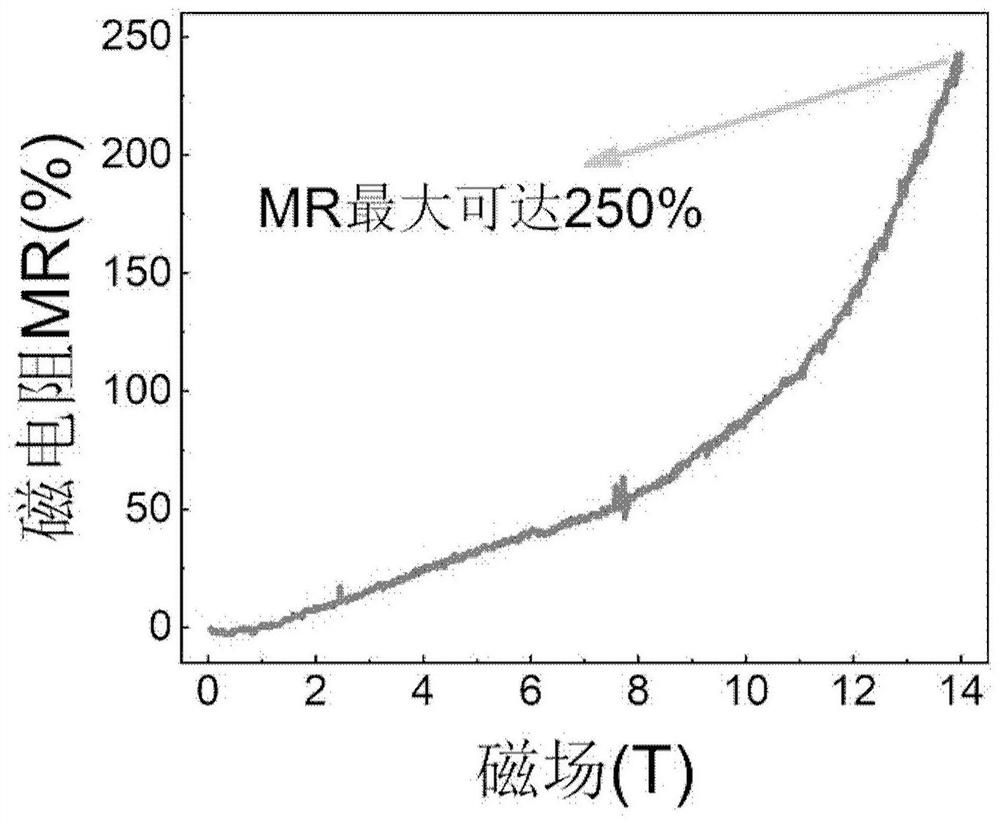
[0085] The measurement method is to use low-temperature strong magnetic field quantum transport equipment for measurement, which can provide a stable ...

Embodiment 2

[0091] Compared with Example 1, the preparation process of the device is the same, the difference is that nanosheets with different thicknesses are used to prepare homojunction devices.

[0092] The lower layer Fe shown in this example 0.021 sn 0.979 S 2 The layer thickness is 12.3nm, about 15 layers;

[0093] The upper layer Fe shown in this example 0.021 sn 0.979 S 2 The layer thickness is 11.5 nm, about 14 layers.

[0094] The annealing temperature and time used in this embodiment are annealing at 200° C. for 60 minutes.


PUM

PropertyMeasurementUnit
thicknessaaaaaaaaaa
thicknessaaaaaaaaaa
thicknessaaaaaaaaaa

Abstract

A homojunction magnetoresistive device of a magnetic two-dimensional semiconductor and its preparation method and application, the homojunction magnetoresistance device includes a silicon layer; a silicon dioxide layer, which is arranged on the silicon layer, and together with the silicon layer as a gate and an insulating layer; the first nanosheet and the second nanosheet are all arranged on the silicon dioxide layer, the first nanosheet and the second nanosheet partially overlap, and the overlapping area forms a vertical structure, the first nanosheet and the second nanosheet The sheets are non-magnetic two-dimensional semiconductor materials doped with transition metal magnetic atoms; and the source and drain are located on the first nanosheet and the second nanosheet respectively. The doping of elements in the present invention is an effective means to control the properties of two-dimensional materials. The doping of non-magnetic materials with transition metal atoms is used to introduce magnetism into non-magnetic materials. This method provides a great opportunity for the development of spintronics. more choices.

Description

technical field [0001] The invention relates to the field of magnetic two-dimensional semiconductors, in particular to a homojunction magnetoresistance device of magnetic two-dimensional semiconductors, a preparation method and application thereof. Background technique [0002] Since graphene was successfully prepared, the development of two-dimensional materials has attracted a lot of attention. Many materials with unique and excellent properties have been discovered and widely studied. For example, transition metal dichalcogenides (TMDCs) have great application potential in the field of optoelectronics because of their excellent optoelectronic properties. In the research on two-dimensional materials, the development of two-dimensional magnetic materials has also attracted the attention of some researchers. [0003] Introducing impurity atoms into materials to change the physical properties of 2D materials is a very effective way to achieve more functionalization of 2D ma...

Claims


Application Information

Patent Timeline
Patent Type & Authority Patents(China)
IPC IPC(8): H01L43/08H01L43/10H01L43/02H01L43/12B82Y30/00
CPCB82Y30/00H10N50/80H10N50/10H10N50/01H10N50/85
Inventor 魏钟鸣房景治黎博廖志敏杨珏晗魏大海宗易昕文宏玉
Owner INST OF SEMICONDUCTORS - CHINESE ACAD OF SCI
Why Eureka
Try Eureka