Seed crystal laying method for producing low-dislocation-density cast single crystal ingot or polycrystalline silicon ingot

A polycrystalline silicon ingot and laying method technology, applied in the direction of single crystal growth, single crystal growth, polycrystalline material growth, etc., can solve the problems of reducing the quality of cast single crystal silicon crystals, reducing the area of ​​single crystals, etc., to achieve the reduction of random grain boundaries, Effect of increasing single crystal area and improving crystal quality

Active Publication Date: 2020-07-24
湖北鑫鸿新能源有限公司
View PDF5 Cites 0 Cited by
  • Summary
  • Abstract
  • Description
  • Claims
  • Application Information

AI Technical Summary

Problems solved by technology

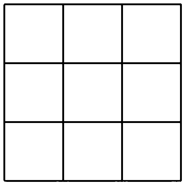
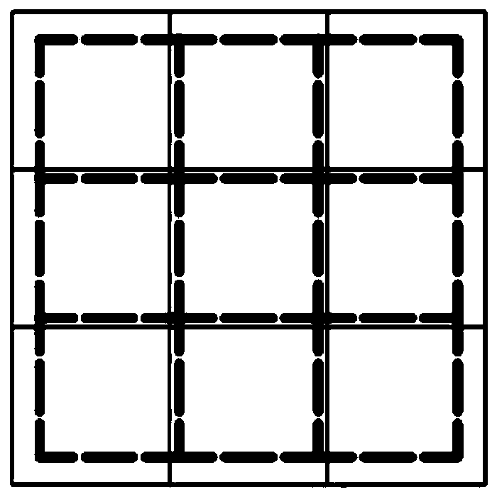
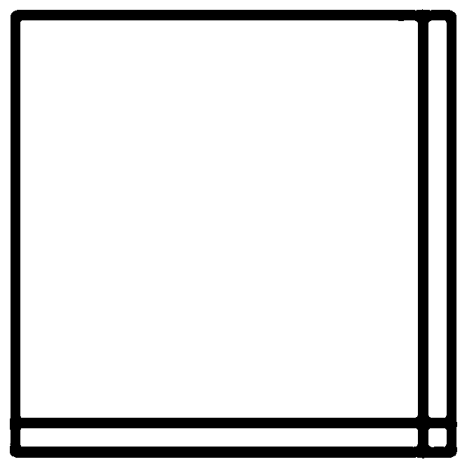
figure 1 Schematic diagram of seed laying for the production of conventional cast single crystals, figure 2 It is a schematic diagram of the square root when producing a conventional cast single crystal, image 3 Schematic diagram of a conventional cast single crystal silicon wafer. It can be seen that the size of the seed block is the same as the size of the silicon wafer. There are few grain boundaries in the cast single crystal silicon wafer. The internal growth of the silicon ingot reduces the single crystal area; due to the lack of grain boundaries, impurities such as carbon, nitrogen, and metals are easy to gather, precipitate, and nucleate locally in the cast single crystal silicon ingot, forming a non-(100) crystal growth direction. The crystal grains reduce the single crystal area; because there are few grain boundaries, there is no grain boundary to block the dislocation crystal, and dislocations are easy to proliferate in large quantities during the crystal growth process, which reduces the crystal quality of cast single crystal silicon

Method used


Image

  • Seed crystal laying method for producing low-dislocation-density cast single crystal ingot or polycrystalline silicon ingot
  • Seed crystal laying method for producing low-dislocation-density cast single crystal ingot or polycrystalline silicon ingot
  • Seed crystal laying method for producing low-dislocation-density cast single crystal ingot or polycrystalline silicon ingot

Examples


specific Embodiment 2

[0084] Referring to the accompanying drawings, in order to clearly see the laying method of the seed crystal, the embodiment only takes the G3 cast single crystal silicon ingot as an example, but the seed laying method provided by the present invention is also applicable to G5, G6, G7, G8 cast single crystal silicon ingots Silicon ingot, a method for laying seed crystals when producing low dislocation density cast single crystal ingots or polycrystalline silicon ingots, comprising the following steps:

[0085] S1: The single crystal square rod A without rounded corners is obtained after removing the skin along the ridge line of the CZ single crystal rod. The cross-sectional size of the single crystal square rod is 160mm×160mm. Figure 18 The big circle in the figure represents a single wafer bar, and the 4 small circles represent ridges;

[0086] S2: After removing the skin along the direction of the ridge line deflection greater than 10° from the CZ single wafer rod, a single...

specific Embodiment 3

[0095] Referring to the accompanying drawings, in order to clearly see the laying method of the seed crystal, the embodiment only takes the G3 cast single crystal silicon ingot as an example, but the seed laying method provided by the present invention is also applicable to G5, G6, G7, G8 cast single crystal silicon ingots Silicon ingot, a method for laying seed crystals when producing low dislocation density cast single crystal ingots or polycrystalline silicon ingots, comprising the following steps:

[0096] S1: The single crystal square rod A without rounded corners is obtained after removing the skin along the ridge line of the CZ single crystal rod. The cross-sectional size of the single crystal square rod is 160mm×160mm. Figure 18 The big circle in the figure represents a single wafer bar, and the 4 small circles represent ridges;

[0097] S2: After removing the skin along the direction of the ridge line deflection greater than 10° from the CZ single wafer rod, a single...

specific Embodiment 4

[0106] Referring to the accompanying drawings, in order to clearly see the laying method of the seed crystal, the embodiment only takes the G3 cast single crystal silicon ingot as an example, but the seed laying method provided by the present invention is also applicable to G5, G6, G7, G8 cast single crystal silicon ingots Silicon ingot, a method for laying seed crystals when producing low dislocation density cast single crystal ingots or polycrystalline silicon ingots, comprising the following steps:

[0107] S1: The single crystal square rod A without rounded corners is obtained after removing the skin along the ridge line of the CZ single crystal rod. The cross-sectional size of the single crystal square rod is 160mm×160mm. Figure 18 The big circle in the figure represents a single wafer bar, and the 4 small circles represent ridges;

[0108] S2: After removing the skin along the direction of the ridge line deflection greater than 10° from the CZ single wafer rod, a single...


PUM


Abstract

The invention discloses a seed crystal laying method for producing a low-dislocation-density cast single crystal ingot or polycrystalline silicon ingot. The seed crystal laying method comprises the following steps: S1, straightly pulling a single crystal silicon rod to remove edge skins to obtain a single crystal square rod without fillets; S2, cutting the single crystal square rod into large seedcrystal blocks; S3, cutting the large seed crystal blocks into small seed crystal blocks or seed crystal strips again; S4, laying the small seed crystal blocks or seed crystal strips at the bottom ofa crucible to form a complete seed crystal layer; S5, placing a primary polycrystalline silicon material and circulating materials such as head and tail edges on the seed crystal layer; S6, putting the crucible filled with the polycrystalline silicon material into an ingot furnace, and obtaining a cast monocrystalline silicon ingot or polycrystalline silicon ingot by adopting a semi-melting process; S7, squaring the silicon ingot, and obtaining a small square ingot after squaring; and S8, slicing the small square ingot to obtain a cast monocrystalline silicon wafer or polycrystalline siliconwafer, wherein the high seed crystals and the short seed crystals are alternately matched during laying so that the contact side surfaces of the high seed crystals and the short seed crystals are perfectly fused, and the probability of dislocation is reduced.

Description

technical field [0001] The invention relates to the technical field of photovoltaic manufacturing, in particular to a method for laying seed crystals when producing low dislocation density cast single crystal ingots or polycrystalline silicon ingots. Background technique [0002] At present, the general steps of producing cast single crystal are as follows: Lay a layer of single crystal seed crystal on the bottom of the crucible, install the head material, tail material, side skin and primary polysilicon material of the normal ingot on the single crystal seed crystal, and use the semi-melting process to obtain Cast single crystal. figure 1 Schematic diagram of seed laying for the production of conventional cast single crystals, figure 2 It is a schematic diagram of the square root when producing a conventional cast single crystal, image 3 Schematic diagram of a conventional cast single crystal silicon wafer. It can be seen that the size of the seed block is the same as t...

Claims


Application Information

Patent Timeline
Patent Type & Authority Applications(China)
IPC IPC(8): C30B13/34C30B29/06B28D5/00C30B13/14
CPCB28D5/00C30B13/14C30B13/34C30B29/06
Inventor 周耐根刘世龙刘淑慧
Owner 湖北鑫鸿新能源有限公司
Why Eureka
Try Eureka