Monocrystal-like silicon ingot, preparation method of monocrystal-like silicon ingot, and monocrystal-like silicon ingot furnace
A technology similar to single crystal silicon and single crystal silicon ingot, applied in the field of semiconductor manufacturing, can solve the problems of affecting the area of casting single crystal single crystal, affecting the life of the minority carrier of the silicon ingot, affecting the electrical properties of the silicon wafer, etc., so as to reduce the enrichment and nucleation. The probability of reducing the concentration of impurities, the effect of simple structure
- Summary
- Abstract
- Description
- Claims
- Application Information
AI Technical Summary
Problems solved by technology
Method used
Image
Examples
preparation example Construction
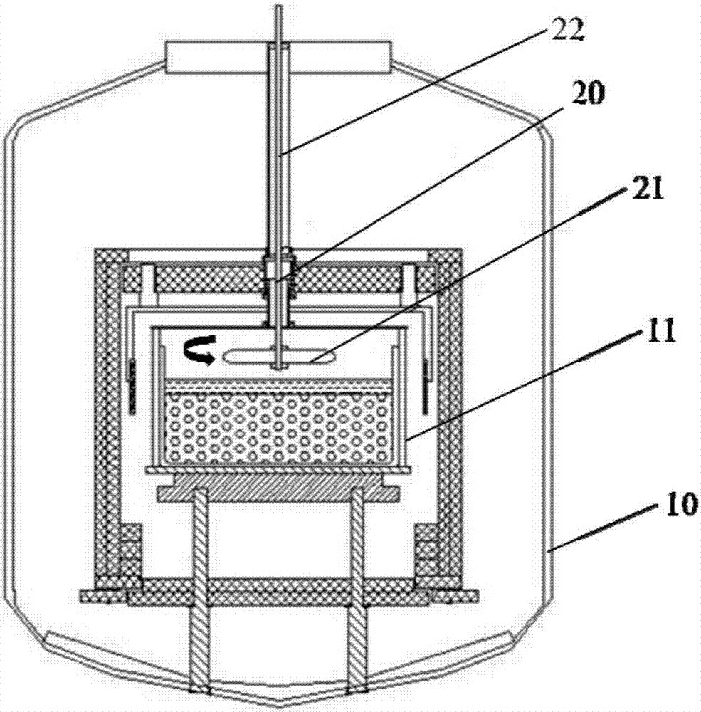
[0032] The first aspect of the embodiment of the present invention provides a method for preparing a kind of single crystal silicon ingot, including:
[0033] Laying seed crystals in the crucible to form a seed crystal layer; setting a silicon melt in a molten state above the seed crystal layer, controlling the temperature at the bottom of the crucible to be lower than the melting point of the seed crystal, so that the seed crystal layer is not completely melt;
[0034] Adjust the thermal field to form a supercooled state, so that the silicon melt begins to grow crystals on the basis of the seed layer; during the crystal growth process, the stirring speed is continuous or intermittent at 1 rpm-60 rpm stirring the silicon melt;
[0035] After all the silicon melt is crystallized, it is annealed and cooled to obtain a quasi-single crystal silicon ingot.
[0036] In the embodiment of the present invention, when entering the crystal growth stage, stirring the silicon melt can en...
Embodiment 1
[0054] A method for preparing a quasi-monocrystalline silicon ingot, comprising:
[0055] (1) Take a quartz crucible (inner diameter 840mm×840mm), lay seed crystals on the bottom of the crucible to form a seed crystal layer with a thickness of 10mm, and then fill various bulk silicon materials above the seed crystal layer. Put the above-mentioned crucible with silicon material into the ingot casting furnace, start the ingot casting program, vacuumize and heat until the melting point of silicon is reached, so that the silicon material slowly melts into a silicon melt.
[0056] (2) Control the temperature at the bottom of the crucible to be lower than the melting point of the seed crystal, so that the seed layer is not completely melted; control the temperature in the crucible to gradually rise in the upward direction perpendicular to the bottom of the crucible to form a temperature gradient, enter the crystal growth stage, and the silicon melt On the basis of the seed crystal, ...
Embodiment 2
[0059] A method for preparing a quasi-monocrystalline silicon ingot, comprising:
[0060] (1) Take a quartz crucible (inner diameter 840mm×840mm), lay seed crystals on the bottom of the crucible to form a seed crystal layer with a thickness of 20mm, and then fill various bulk silicon materials above the seed crystal layer. Put the above-mentioned crucible with silicon material into the ingot casting furnace, start the ingot casting program, vacuumize and heat until the melting point of silicon is reached, so that the silicon material slowly melts into a silicon melt.
[0061] (2) Control the temperature at the bottom of the crucible to be lower than the melting point of the seed crystal, so that the seed layer is not completely melted; control the temperature in the crucible to gradually rise in the upward direction perpendicular to the bottom of the crucible to form a temperature gradient, enter the crystal growth stage, and the silicon melt On the basis of the seed crystal, ...
PUM
| Property | Measurement | Unit |
|---|---|---|
| length | aaaaa | aaaaa |
| thickness | aaaaa | aaaaa |
| distance | aaaaa | aaaaa |
Abstract
Description
Claims
Application Information


