A micro-Raman combined with photoluminescence detection device and method for a micro LED chip

A photoluminescence, micro-Raman technology, applied in the direction of measurement devices, Raman scattering, fluorescence/phosphorescence, etc., can solve the problem of greatly increasing the frame rate, achieve increased scanning speed, improved suppression level, and make up for the lack of accuracy Effect

Active Publication Date: 2021-06-01
PEKING UNIV
View PDF12 Cites 0 Cited by
  • Summary
  • Abstract
  • Description
  • Claims
  • Application Information

AI Technical Summary

Problems solved by technology

However, the method of multi-focus parallel imaging has not been used in confocal Raman spectroscopy instruments, and the frame rate of current commercial instruments needs to be greatly improved.

Method used


Image

  • A micro-Raman combined with photoluminescence detection device and method for a micro LED chip
  • A micro-Raman combined with photoluminescence detection device and method for a micro LED chip
  • A micro-Raman combined with photoluminescence detection device and method for a micro LED chip

Examples


Embodiment 1

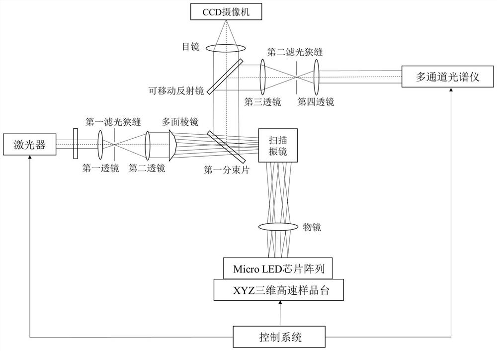
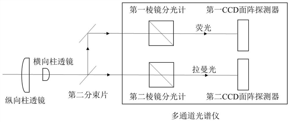
[0044] In this example, Stokes Raman was used in combination with fluorescence measurements. The general Raman test is aimed at the measurement of the vibrational Stokes peak, and the photon wavelength of the Raman scattering of the test sample is within 30nm higher than the wavelength of the incident light.

[0045] In this embodiment, the micro LED chip array is a 6-inch epitaxial wafer, and about 20 million LED chip units with a size of 20 μm are prepared. Set the scanning range of each frame to 400μm×400μm, then there are 20×20=400 LED chip units in one frame, and the single-point scanning frame rate is 10 frames per second. If one-dimensional laser dot matrix illumination is used, the excitation light If there are 20 spots, the frame rate will reach 200 frames per second. The number of LED chip units that can be measured in one second reaches 80,000, and in one hour it can reach 288 million. It can measure more than 14 pieces of 6-inch micro LED chip arrays, which is muc...

Embodiment 2

[0050] In this example, anti-Stokes Raman was used in combination with fluorescence measurements. The anti-Stokes Raman test is aimed at the measurement of the vibrational anti-Stokes peak, and the photon wavelength of the Raman scattering of the test sample is smaller than the wavelength of the excitation light. The intensity of anti-Stokes Raman scattering is an order of magnitude lower than that of Stokes Raman, but because the spectral range avoids the range of photoluminescence, the signal-to-noise ratio can be significantly improved.

[0051] In this embodiment, the micro LED chip array is a 6-inch epitaxial wafer, and about 20 million LED chip units with a size of 20 μm are prepared. Set the scanning range of each frame to 400μm×400μm, then there are 20×20=400 LED chip units in one frame, and the single-point scanning frame rate is 10 frames per second. If one-dimensional laser dot matrix illumination is used, the excitation light If there are 20 spots, the frame rate ...


PUM


Abstract

The invention discloses a micro-Raman combined photoluminescence detection device and a method for a micro LED chip. The present invention combines a polygonal prism with a CCD area array detector, so that the one-dimensionally arranged light spot array is received by a two-dimensional area array CCD area array detector, and the spectral distribution of each light spot is obtained without complex laser frequency modulation and Signal demodulation technology, which can obtain optical properties and electrical properties, greatly improves the scanning speed; adopts Brewster angle incidence, double cylindrical lens beam shaping and prism spectrometer to reduce the sub-peak spurious spectrum caused by grating, so that the stray The suppression level of scatter spectrum is significantly improved; the combination of photoluminescence detection and Raman detection, photoluminescence detection provides luminescence wavelength and brightness information, and Raman detection provides electrical properties, which makes up for the lack of accuracy of photoluminescence detection.

Description

technical field [0001] The invention relates to the field of semiconductor devices, in particular to a micro-Raman combined photoluminescence detection device and a detection method for a micro LED chip. Background technique [0002] At present, the miniaturization trend of light-emitting diode (LED) chips is obvious. In the display field, the chip size of micro LED is reduced to less than 50 microns. Compared with LCD and OLED, it has obvious advantages in terms of brightness, resolution, energy consumption and response speed. Advantage. In order to ensure the production yield of micro LED chips, detection is a crucial link. Usually, the main parameters of LED chip detection include dominant wavelength, brightness, forward bias voltage, reverse leakage, short circuit and open circuit, etc. Photoluminescence (Photoluminescence; PL) scanning mapping (mapping) technology is a commonly used detection method. Photoluminescence detection can directly give the light-emitting wave...

Claims


Application Information

Patent Timeline
Patent Type & Authority Patents(China)
IPC IPC(8): G01N21/65G01N21/64
CPCG01N21/64G01N21/6402G01N21/645G01N21/6454G01N21/6458G01N21/6489G01N21/65G01N21/658G01N2021/6417G01N2021/6471G01N2021/6478G01N2021/6495G01N2021/655
Inventor 陈志忠潘祚坚焦飞张树霖康香宁陈怡帆詹景麟陈毅勇聂靖昕沈波
Owner PEKING UNIV
Why Eureka
Try Eureka