Grain production method for twice thinning by front cutting

A production method and grain technology, applied in the direction of electrical components, semiconductor/solid-state device manufacturing, circuits, etc., can solve the problems of increasing grain production cost, grain scrapping damage, grain damage, etc., to shorten cutting time, control The effect of reducing production cost and improving the qualified rate of finished products

Active Publication Date: 2020-07-24
绍兴同芯成集成电路有限公司
View PDF5 Cites 0 Cited by
  • Summary
  • Abstract
  • Description
  • Claims
  • Application Information

AI Technical Summary

Problems solved by technology

At present, the wafer is bonded to the glass carrier, and the glass carrier is used to transfer the wafer for wafer thinning, backside yellowing, ion implantation, metal deposition and other processes, and finally the die is cut on the die film frame And subsequent testing and packaging, it is necessary to implement yellow light, ion implantation, and metal deposition processes on the back of the thinned wafer before the wafer cutting process is performed, but the wafers that are thinned to 20 microns to 80 microns are used for cutting grains. At the same time, due to the warpage of the thin wafer, and the metal deposition of the wafer has been completed, when the external force is cut, the changing stress during cutting will easily cause the wafer to crack, and the grain cannot be reworked and scrapped. Most of the prior art is cut before cutting. Complete back yellow light, ion implantation, metal deposition process, it is very easy to cause damage to the grain during cutting, which increases the production cost of the grain

Method used


Image

  • Grain production method for twice thinning by front cutting
  • Grain production method for twice thinning by front cutting
  • Grain production method for twice thinning by front cutting

Examples


Embodiment 1

[0048] A method for producing grains by front-side cutting twice for thinning, the production method comprising the following steps:

[0049] S1: front cut

[0050] The wafer 1 is cut by means of diamond cutting, and the die 4 is cut from the front side of the die 4 to a position of 1.05X, where X is the estimated final thickness of the wafer 1 after thinning.

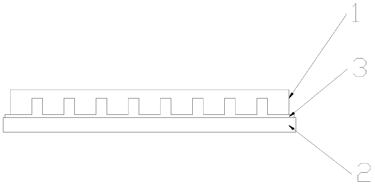
[0051] S2: fixed once

[0052] Use adhesive 3 to bond the cut front side of wafer 1 on glass carrier 2, such as figure 1 As shown, the adhesive 3 bonds the wafer 1 and the glass carrier 2 together by UV bonding, the temperature requirement is 50-200° C., and the use time is less than 30 minutes.

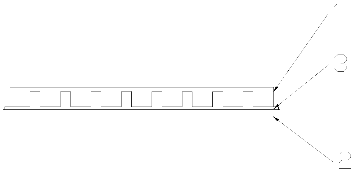
[0053] S3: one thinning

[0054] Thinning the cut backside by grinding, such as figure 2 As shown, the thickness of one thinning is 1.01Y, Y=1.05X.

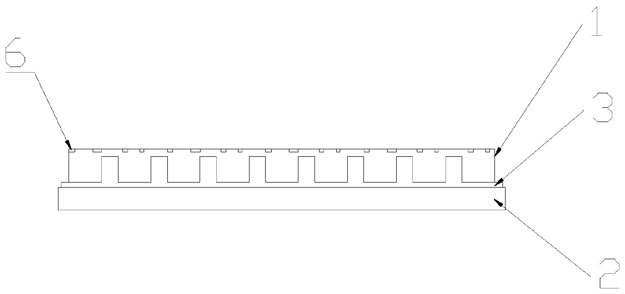
[0055] S4: intermediate process

[0056] Yellow light on the back side, ion implantation, ion implantation layer 6 is formed on the back side of the crystal grain 4, such...

Embodiment 2

[0070] A method for producing grains by front-side cutting twice for thinning, the production method comprising the following steps:

[0071] S1: front cut

[0072] The wafer 1 is cut by laser cutting, and the die 4 is cut from the front side of the die 4 to a position of 1.2X, where X is the estimated final thickness of the wafer 1 after thinning.

[0073] S2: fixed once

[0074]Use the adhesive 3 to bond the cut front of the wafer 1 to the glass carrier 2. The adhesive bonds the wafer 1 and the glass carrier 2 together by heating and bonding. The temperature requirement is 150-300°C. The time of use is 30 minutes or less.

[0075] S3: one thinning

[0076] Thinning is performed on the cut back side by etching, and the thickness of the first thinning is 1.1Y, Y=1.2X.

[0077] S4: intermediate process

[0078] Backside yellow light, ion implantation, ion implantation layer 6 is formed on the backside of crystal grain 4, photoresist removal, annealing process.

[0079] S5...

Embodiment 3

[0092] A method for producing grains by front-side cutting twice for thinning, the production method comprising the following steps:

[0093] S1: front cut

[0094] The wafer 1 is cut by means of plasma cutting, and the die 4 is cut from the front side of the die 4 to a position of 1.3X, where X is the estimated final thickness of the wafer 1 after thinning.

[0095] S2: fixed once

[0096] Use the adhesive 3 to bond the cut front of the wafer 1 to the glass carrier 2. The adhesive 3 bonds the wafer 1 and the glass carrier 2 together by heating and bonding, and the temperature requirement is 150-300°C , the use time is less than 30 minutes.

[0097] S3: one thinning

[0098] Thinning is performed on the cut back surface by etching, and the thickness of the first thinning is 1.2Y, Y=1.3X.

[0099] S4: intermediate process

[0100] Backside yellow light, ion implantation, ion implantation layer 6 is formed on the backside of crystal grain 4, photoresist removal, annealing p...


PUM


Abstract

The invention discloses a crystal grain production method for twice thinning through front cutting. The production method comprises the steps of front cutting, primary fixing, primary thinning, an intermediate process, secondary thinning, adhesive removal, a metal deposition process, secondary fixing, separation from a glass carrier plate and solvent cleaning. According to the invention, through cutting, primary fixing, primary thinning, the intermediate process, secondary thinning, adhesive removal, the metal deposition process, secondary fixing, separation from the glass carrier plate and solvent cleaning, a wafer is subjected to front cutting and twice thinning to obtain crystal grains; a traditional one-time cutting mode is replaced; damage to crystal grains caused by cutting is reduced; the finished product percent of pass of the crystal grains is increased; the cutting time of a single qualified crystal grain is shortened; a traditional process of completing back yellow light, ion implantation and metal deposition before cutting is replaced; and the production cost of the crystal grains is easily controlled.

Description

technical field [0001] The invention relates to a production method, in particular to a crystal grain production method with double-thinning front cutting. Background technique [0002] An ultra-thin wafer, generally with a thickness of 20-250 microns, is used for MOSFET and IGBT power devices and 3-D devices. At present, the wafer is bonded to the glass carrier, and the glass carrier is used to transfer the wafer for wafer thinning, backside yellowing, ion implantation, metal deposition and other processes, and finally the die is cut on the die film frame And subsequent testing and packaging, it is necessary to implement yellow light, ion implantation, and metal deposition processes on the back of the thinned wafer before the wafer cutting process is performed, but the wafers that are thinned to 20 microns to 80 microns are used for cutting grains. At the same time, due to the warpage of the thin wafer, and the metal deposition of the wafer has been completed, when the ext...

Claims


Application Information

Patent Timeline
IPC IPC(8): H01L21/304H01L21/78H01L21/302
CPCH01L21/304H01L21/78H01L21/302
Inventor 严立巍李景贤陈政勋
Owner 绍兴同芯成集成电路有限公司
Why Eureka
Try Eureka