Embedded chip package and manufacturing method thereof

An embedded chip and chip packaging technology, applied in semiconductor/solid-state device manufacturing, electrical components, electrical solid-state devices, etc., can solve problems such as easy peeling, reduced lifespan, and long operation process, so as to simplify the process steps and avoid damage Risk, the effect of reducing production costs

Inactive Publication Date: 2020-08-18
ZHUHAI ADVANCED CHIP CARRIERS & ELECTRONICS SUBSTRATE SOLUTIONS TECH
View PDF7 Cites 3 Cited by
  • Summary
  • Abstract
  • Description
  • Claims
  • Application Information

AI Technical Summary

Problems solved by technology

[0008] In the case of exposing openings through laser drilling on conventional packaging materials, the energy of the laser is likely to generate stress inside the chip or device, which is likely to cause damage to the chip or device, so it is not suitable for embedding of bare chips / devices without conductive pillars
[0009] In the case of exposing openings by dry etching on conventional packaging materials, it is difficult to achieve small holes, and even for large openings, there are still long work processes, low process output, limited product design, poor uniformity, and short life. shortcoming
In addition, dry etching usually needs to grind and thin the packaging material, and the panel frame is usually made of glass fiber composite material (such as BT), so it has to face the problem of glass fiber exposure after grinding, and the glass fiber exposure will Limit the ability of fine lines, such as poor bonding of copper on glass fibers and easy peeling; and exposed glass fibers are easy to form electromigration channels, resulting in electrical performance failure and reduced lifespan

Method used


Image

  • Embedded chip package and manufacturing method thereof
  • Embedded chip package and manufacturing method thereof
  • Embedded chip package and manufacturing method thereof

Examples


Embodiment Construction

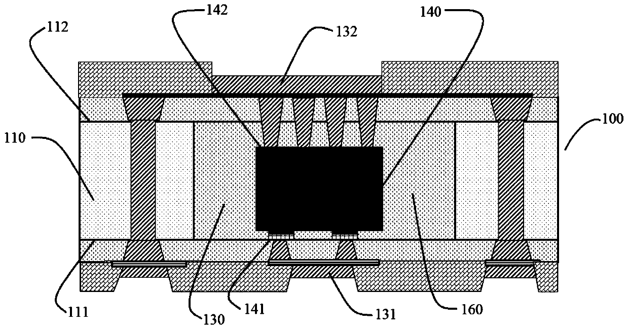
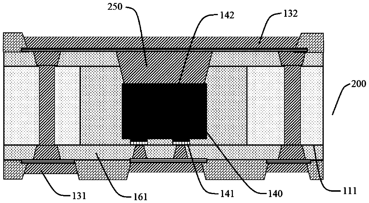
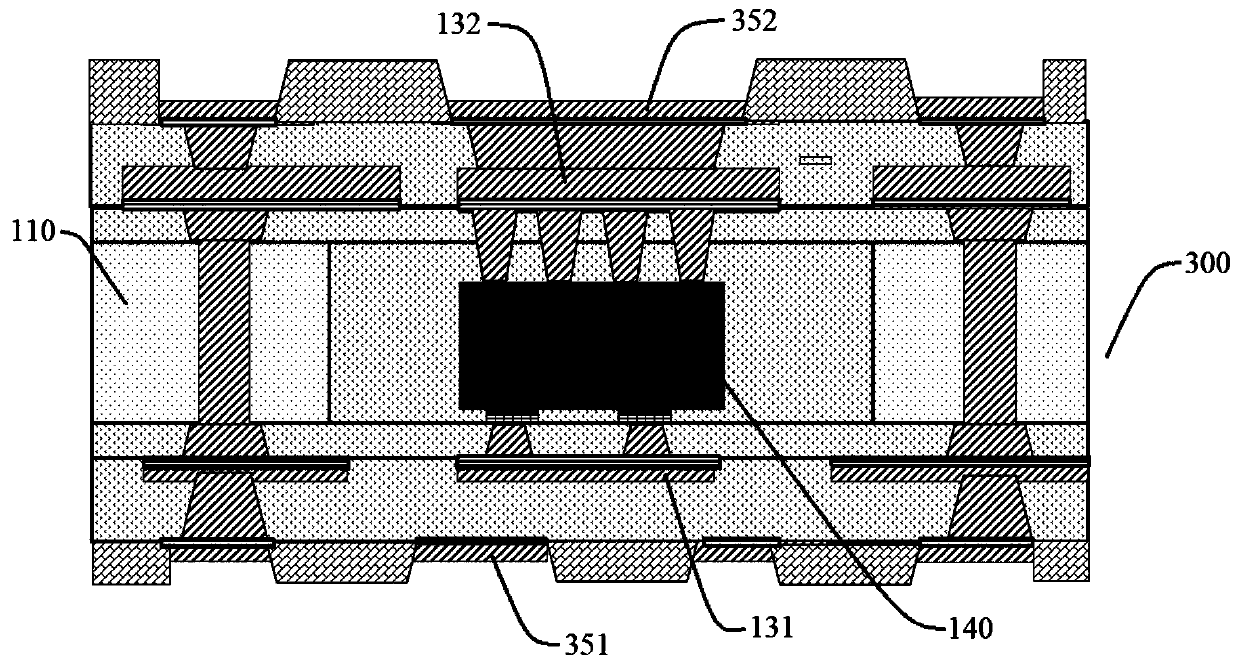
[0049] The invention relates to embedded chip packaging, which is characterized in that the chip and the frame are embedded in the photosensitive polymer dielectric material as the packaging material, an opening is directly formed on the back of the chip and metal such as copper is deposited, and at the same time, it is also passed through the terminal surface of the chip. The photosensitive polymer dielectric material is arranged to produce openings to form metal pillars that conduct the chip terminals, thereby forming a double-sided conduction or heat dissipation structure of the chip.

[0050] The photosensitive polymer dielectric material used in the present invention mainly includes polyimide photosensitive resin and polyphenylene ether photosensitive resin, such as Microsystems HD-4100, Hitachi PVF-02 and the like.

[0051] The metal posts formed on the surface of the chip terminals are used to connect the chip terminals with the first wiring layer. Metal pillars formed ...


PUM


Abstract

The invention discloses an embedded chip package and a manufacturing method thereof. The chip package includes at least one chip and a frame surrounding the at least one chip, the chip is provided with a terminal surface and a back surface which are separated by the height of the chip, and the height of the frame is equal to or larger than the height of the chip, wherein a gap between the chip andthe frame is completely filled with a photosensitive polymer dielectric material, a terminal surface of the chip is coplanar with the frame, a first wiring layer is arranged on the terminal surface of the chip, and a second wiring layer is arranged on the back surface of the chip. The invention further discloses a manufacturing method of the embedded chip package.

Description

technical field [0001] The invention relates to chip packaging, in particular to embedded chip packaging and a manufacturing method thereof. Background technique [0002] With the vigorous development of the electronic industry, electronic products have gradually entered the era of multi-function, miniaturization and high performance. The increasing demand for high density, multi-function and miniaturization has brought new challenges to both packaging and substrates, and many new packaging technologies have emerged, including embedded packaging technology. [0003] Embedded packaging technology is to embed passive components such as resistors, capacitors, inductors, or even active components such as ICs into the packaging substrate. This approach can shorten the length of the lines between components, improve electrical characteristics, and improve effective Printed circuit board packaging area, reducing a large number of solder joints on the printed circuit board surface,...

Claims


Application Information

Patent Timeline
Patent Type & Authority Applications(China)
IPC IPC(8): H01L23/29H01L23/31H01L21/50H01L21/56
CPCH01L23/293H01L23/3107H01L21/50H01L21/56H01L2224/18H01L21/568H01L21/6835H01L2221/68359H01L2221/68381H01L21/561H01L23/5389H01L23/49827H01L21/486H01L24/86H01L23/041H01L23/36H01L23/481H01L23/485H01L24/96
Inventor 陈先明冯进东黄本霞冯磊王闻师
Owner ZHUHAI ADVANCED CHIP CARRIERS & ELECTRONICS SUBSTRATE SOLUTIONS TECH
Why Eureka
Try Eureka