Method for inspecting microwave capability of plate-type PECVD
An inspection board and microwave technology, which is applied in the direction of material analysis, instruments, and electrical components using microwave means, can solve the problems of inability to find microwave capabilities, weakened microwave capabilities, and increased production costs, so as to solve the problem of poor color quality and poor quality. Improve the comparison accuracy and improve the effect of accuracy
- Summary
- Abstract
- Description
- Claims
- Application Information
AI Technical Summary
Problems solved by technology
Method used
Image
Examples
Embodiment 1
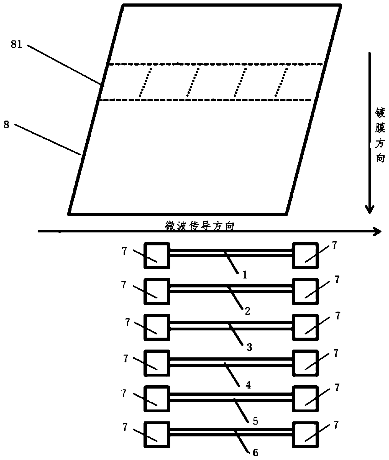
[0037] The invention provides a method for inspecting the microwave capability of plate-type PECVD, which uses the P-type silicon wafer as the substrate after the processes of texturing, diffusion, and removal of peripheral PN junctions;
[0038] see figure 1 , based on the operation of the single-end microwave system 7 in a single normal quartz tube, the coating parameters of the substrate are designed so that the film thickness on the substrate reaches the range of 50-100nm, so that the detection tool can be used to identify and detect the film on the test piece Thickness and refractive index, in the present invention, all embodiments all adopt unified coating parameters, so that follow-up comparative analysis, the coating parameters during coating in the present invention are: microwave system 7 opening ends (testing end) in the quartz tube to be measured ) power is 3500W, all the other quartz tubes and the microwave system 7 power at the opposite end of the test end in the...
Embodiment 2
[0053] Different from Example 1, this example also detected and recorded 1A test piece, 2A test piece, 3A test piece, 4A test piece, 5A test piece, 6A test piece, 1B test piece, 2B test piece, 3B test piece The refractive index of the test piece, 4B test piece, 5B test piece, and 6B test piece, judge whether there is any abnormality in the special gas flowmeter of the quartz tube through the relationship between the refractive index and the film thickness, and one of the abnormality of the special gas flowmeter is the performance It is: the coating thickness of the test piece sample corresponding to the quartz tube is negatively correlated with the refractive index, but the coating thickness is obviously thicker or thinner than the test piece samples corresponding to other quartz tubes, and the overall thickness is thicker or thinner. It means that the film thickness of all the test pieces in the test column 81 and the film thickness of each test piece in other test columns hav...
Embodiment 3
[0059] The difference from Example 2 is that this test uses N-type silicon after texturing, diffusion, removal of the back and surrounding PN junctions, removal of the back PSG and front BSG, and superposition of aluminum oxide deposition, thermal oxidation and SE laser processes. The sheet is used as the substrate, and the film thickness and refractive index test results of the generated test sheet sample 8 are shown in Table 3:
[0060] table 3
[0061] sample name Film thickness (nm) Refractive index 1B test piece sample 82.7 2.13 2B test piece sample 80.3 2.15 3B test piece sample 83.9 2.10 4B test piece sample 70.2 2.19 5B test piece sample 84.6 2.09 6B test piece sample 85.8 2.08
[0062] In this embodiment, it is found that although the same coating parameters are used, and the film thickness of each test piece sample is negatively correlated with the refractive index, the film thickness of the 4B test piece sa...
PUM
| Property | Measurement | Unit |
|---|---|---|
| thickness | aaaaa | aaaaa |
| thickness | aaaaa | aaaaa |
| thickness | aaaaa | aaaaa |
Abstract
Description
Claims
Application Information
 - R&D
- Intellectual Property
- Life Sciences
- Materials
- Tech Scout
- Unparalleled Data Quality
- Higher Quality Content
- 60% Fewer Hallucinations
Browse by: Latest US Patents, China's latest patents, Technical Efficacy Thesaurus, Application Domain, Technology Topic, Popular Technical Reports.
© 2025 PatSnap. All rights reserved.Legal|Privacy policy|Modern Slavery Act Transparency Statement|Sitemap|About US| Contact US: help@patsnap.com


