Structure of intrinsic passivation layer of silicon heterojunction solar cell and manufacturing method of structure

A solar cell and silicon heterojunction technology, applied in the field of solar cells, can solve the problems of mutual constraints of high passivation performance and low series resistance, high passivation performance and low parasitic absorption can not be achieved at the same time, to improve the overall photoelectric characteristics, High short-circuit current, life-enhancing effects

Active Publication Date: 2020-09-04
ZHONGWEI NEW ENERGY CHENGDU CO LTD
View PDF8 Cites 2 Cited by
  • Summary
  • Abstract
  • Description
  • Claims
  • Application Information

AI Technical Summary

Problems solved by technology

[0007] In view of the problems involved in the background technology, the purpose of the present invention is to provide an intrinsic passivation layer structure and a manufacturing method of a silicon heterojunc

Method used


Image

  • Structure of intrinsic passivation layer of silicon heterojunction solar cell and manufacturing method of structure
  • Structure of intrinsic passivation layer of silicon heterojunction solar cell and manufacturing method of structure
  • Structure of intrinsic passivation layer of silicon heterojunction solar cell and manufacturing method of structure

Examples


Embodiment 1

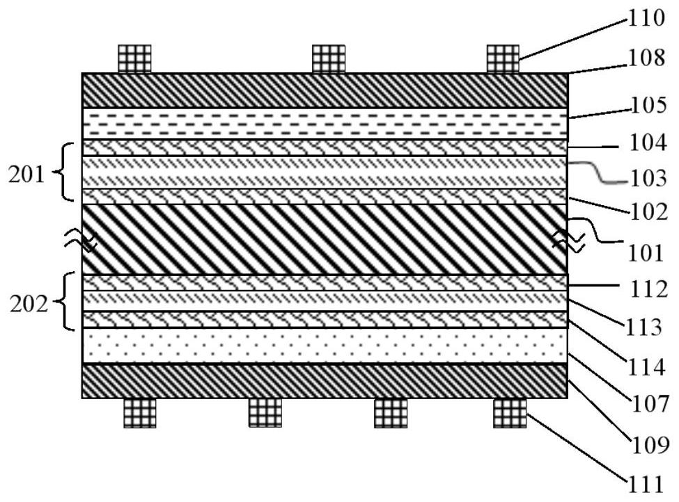
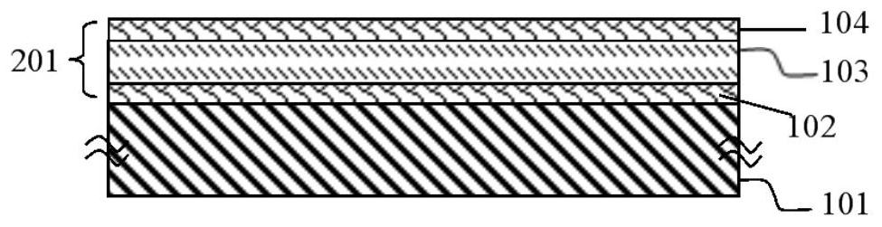
[0046] refer to figure 1 , figure 2 , Figure 4 , using the plasma-enhanced chemical vapor method to deposit the intrinsic silicon-based thin film passivation layer 201 with a specific structure and the structure and manufacturing method of the SHJ solar cell, the implementation method has the following steps:

[0047] (1) Prepare the n-type crystalline silicon substrate: adopt conventional texturing and cleaning steps to obtain a textured crystalline silicon substrate with a clean surface;

[0048] (2) Deposit intrinsic silicon-based film passivation layer on the first light-receiving surface: utilize plasma-enhanced chemical vapor phase method to deposit each layer of silicon film, such as figure 1 As shown, first, a layer of i-a-Si:H with a thickness of about 4 nm is deposited on the upper surface of the solar cell; then, a layer of wide bandgap silicon oxide i-SiO with a thickness of about 8 nm is grown x (x=1, 2, 3...) layer; Next, grow a layer of i-a-Si with a thickn...

Embodiment 2

[0059] refer to figure 2 and image 3 As shown, the first light-receiving surface intrinsic silicon-based passivation layer 201 and the second light-receiving surface intrinsic silicon-based passivation layer 202 with a specific structure are deposited by the hot filament chemical vapor method, and the SHJ solar cell structure with high double-faciality And the production method, the implementation method is as follows:

[0060] (1) Prepare the n-type crystalline silicon substrate: adopt conventional texturing and cleaning steps to obtain a textured crystalline silicon substrate with a clean surface;

[0061] (2) Depositing the intrinsic silicon-based passivation layer 201 on the first light-receiving surface by the hot filament chemical vapor method: as image 3 As shown, first, a layer of i-a-Si:H with a thickness of about 1 nm is deposited on the surface of the first light-receiving surface of the silicon wafer; then, a layer of wide-bandgap silicon oxide i-SiC with a th...


PUM

PropertyMeasurementUnit
Thicknessaaaaaaaaaa
Thicknessaaaaaaaaaa

Abstract

The invention relates to the technical field of solar cells, in particular to a structure of an intrinsic passivation layer of a silicon heterojunction solar cell and a manufacturing method of the structure. The structure comprises a first light receiving surface arranged over a monocrystalline silicon wafer substrate and a second light receiving surface arranged under the monocrystalline siliconwafer substrate; the intrinsic silicon-based thin film passivation layer is of a three-layer composite structure at least in the first light receiving surface or in both the first light receiving surface and the second light receiving surface; in the three-layer composite structure, the first layer and the third layer are intrinsic doped hydrogenated amorphous silicon layers respectively, and thesecond layer is a wide-band gap intrinsic hydrogenated amorphous SiAx: H layer arranged between the first layer and the third layer. The manufacturing method comprises the following steps: depositingthe amorphous silicon layer on the light receiving surface of the crystalline silicon substrate; growing a wide band gap silicon-based i-SiAx layer; and growing an amorphous silicon layer to form theintrinsic silicon-based passivation layer. The problems that high passivation performance and low parasitic absorption cannot be obtained at the same time and the high passivation performance and lowseries resistance restrict each other are solved; and according to the intrinsic silicon-based passivation layer, the recombination rate of the surface of crystalline silicon can be reduced, and incident light reaching the absorption layer can be improved by using a wide band gap.

Description

technical field [0001] The invention relates to the technical field of solar cells, in particular to a structure of an intrinsic passivation layer of a silicon heterojunction solar cell and a manufacturing method thereof. Background technique [0002] With the development of economy and society, the extensive use of conventional fossil energy has not only led to serious environmental pollution problems, but also the increasingly scarce resources. Vigorously developing and utilizing clean energy has become a powerful guarantee for the sustainable development of human society. The sun is inexhaustible, clean and pollution-free, and is an ideal green energy source. Solar cells directly convert light energy into electrical energy, which is an important way to utilize the sun. [0003] Silicon heterojunction (SHJ) solar cells passivate the surface defect states of crystalline silicon (c-Si) with the help of hydrogenated amorphous silicon thin film (a-Si:H), which can achieve ult...

Claims


Application Information

Patent Timeline
IPC IPC(8): H01L31/0747H01L31/0216H01L31/20
CPCH01L31/0747H01L31/02167H01L31/202Y02E10/50Y02P70/50
Inventor 张丽平刘正新韩安军孟凡英石建华杜俊霖蓝仕虎闫涛罗洁
Owner ZHONGWEI NEW ENERGY CHENGDU CO LTD
Why Eureka
Try Eureka