V-band CMOS power amplifier

A power amplifier and band technology, which is applied in the field of V-band power amplifiers, can solve the problems of limiting the output power of single-tube amplifiers, increasing the difficulty of amplifier matching circuits, and reducing the optimal load impedance, so as to achieve good input and output matching and reduce breakdown Risk, the effect of high output power

Active Publication Date: 2020-09-04
UNIV OF ELECTRONICS SCI & TECH OF CHINA
View PDF11 Cites 2 Cited by
  • Summary
  • Abstract
  • Description
  • Claims
  • Application Information

AI Technical Summary

Problems solved by technology

[0003] The principle of the silicon CMOS amplifier is to use the transconductance of the gate to amplify the signal, but due to the disadvantage of the low breakdown voltage of the silicon-based process, the output power of the single-transistor amplifier is limited.
In order to increase the output power of the amplifier, multi-tube parallel synthesis is usually used, such as the literature "J.N.Chang and Y.

Method used


Image

  • V-band CMOS power amplifier
  • V-band CMOS power amplifier
  • V-band CMOS power amplifier

Examples


Embodiment Construction

[0033] In order to illustrate the technical solutions of the present invention, the embodiments are described in detail below in conjunction with the accompanying drawings.

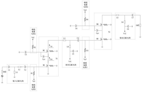
[0034] This embodiment provides a V-band CMOS power amplifier, the circuit principle diagram of which is as follows figure 1 As shown, a two-stage amplifier circuit structure is adopted, which are cascode structures T1 and T2 respectively, including: input matching circuit, inter-stage matching circuit, output matching circuit, cascode structure T1 and T2, gate bias Circuits 1 to 4; where:

[0035] The input matching circuit is composed of a parallel short circuit L1 and a series transmission line L2;

[0036] The inter-stage matching circuit is composed of a series transmission line L3, a parallel stub line L4 and a bypass capacitor C5. At the same time, the drain bias Vd1 is fed in from the radio frequency short-circuit point of the inter-stage matching circuit; the radio frequency short-circuit point ...


PUM


Abstract

The invention belongs to the technical field of millimeter wave communication, and particularly provides a V-band CMOS power amplifier which is used for solving the problems that in the prior art, thecircuit structure is complex, the chip area is large, and the design difficulty of an amplifier matching circuit is large. The amplifier comprises an input matching circuit, a first-stage amplification circuit, an inter-stage matching circuit, a second-stage amplification circuit and an output matching circuit which are connected in sequence, wherein the two stages of amplification circuits are formed by stacking transistors M1 (or M3) and M2 (or M4) respectively; the transistor stacking mode is simple in structure, the breakdown risk of the transistors can be effectively reduced, and the optimal power amplifier saturation output power is obtained; meanwhile, the transistor stacking structure can greatly improve the stability of the millimeter wave power amplification circuit; in addition, the input and output matching circuits in a grounding coplanar waveguide form can further improve the gain and the output power of the millimeter wave amplifier while realizing good input and outputmatching of the stacked transistors in a millimeter wave frequency band.

Description

technical field [0001] The invention belongs to the technical field of millimeter wave communication, and specifically provides a V-band power amplifier based on a CMOS process. Background technique [0002] With the huge increase in the mobile Internet's demand for wireless communication rates, high-speed millimeter-wave wireless communication has become a research hotspot in the field of communication; compared with traditional low-band communication systems, millimeter-wave communication systems have an extremely wide operating frequency band, so the transmission speed of the system It can easily reach the Gbps level. Millimeter-wave power amplifiers are one of the core devices in millimeter-wave communication systems. At present, most of them are manufactured using high-cost III-V compound semiconductor processes. In recent years, with the continuous development and maturity of silicon CMOS technology, its feature size has been continuously reduced, and the cut-off freq...

Claims


Application Information

Patent Timeline
IPC IPC(8): H03F3/20
CPCH03F3/20Y02D30/70
Inventor 杨自强行苗杨涛
Owner UNIV OF ELECTRONICS SCI & TECH OF CHINA
Why Eureka
Try Eureka