Cutting method of GaAs-based LED chip

A technology of LED chip and cutting method, applied in electrical components, circuits, semiconductor devices, etc., can solve problems such as unrealizable structure and photoresist deformation, and achieve the effects of avoiding excessive temperature, ensuring integrity, and convenient removal.

Active Publication Date: 2020-09-08
SHANDONG INSPUR HUAGUANG OPTOELECTRONICS
View PDF5 Cites 0 Cited by
  • Summary
  • Abstract
  • Description
  • Claims
  • Application Information

AI Technical Summary

Problems solved by technology

This method etches from the front of the COW, which requires a thicker photoresist or other medium as a mask, and the etching depth is affected by the thickness of the photoresist or other dielectric mask, so it is not suitable for deep etching. After a long time of etching , the temperature in the reaction chamber will cause the deformation of the photoresist, and the final deformation will be transferred to the chip, and the preset structure cannot be realized.

Method used


Image

  • Cutting method of GaAs-based LED chip
  • Cutting method of GaAs-based LED chip
  • Cutting method of GaAs-based LED chip

Examples


Embodiment 1

[0052] A method for cutting a GaAs-based LED chip, the specific steps comprising:

[0053] (1) COW, the pre-process semi-finished product of GaAs-based LED chips, the P side where the P electrode 2 on the epitaxial layer 1 of the COW is also called the front side of the COW, and the structure is as follows figure 1 As shown, the COW is ground to 120 μm, and the schematic diagram of the interface structure after COW grinding is shown in image 3 shown.

[0054] (2) On the N side of COW, also known as the back side of COW, vapor-deposit ohmic contact metal film layer 3, which is a composite ohmic contact metal film layer of Ge / Au, and make ohmic contact metal film layer on the N side of COW. The schematic diagram of the interface structure after layer 3 is shown in Figure 4 As shown, the thickness of the ohmic contact metal film layer 3 is 0.5 μm.

[0055] (3) Utilize the double-sided positioning photolithography process to make a chip dicing line corresponding to the P side...

Embodiment 2

[0062] According to the cutting method of a GaAs-based LED chip provided in Embodiment 1, the difference is that:

[0063] In step (1), the pre-process semi-finished product COW of the GaAs-based LED chip is ground to 160 μm.

[0064] In step (2), the ohmic contact metal film layer 3 is vapor-deposited on the N surface of the semi-finished COW. The material of the ohmic contact metal film layer 3 is a composite metal film layer of Ni / Ge / Au, and the thickness of the ohmic contact metal film layer 3 is 5 μm. .

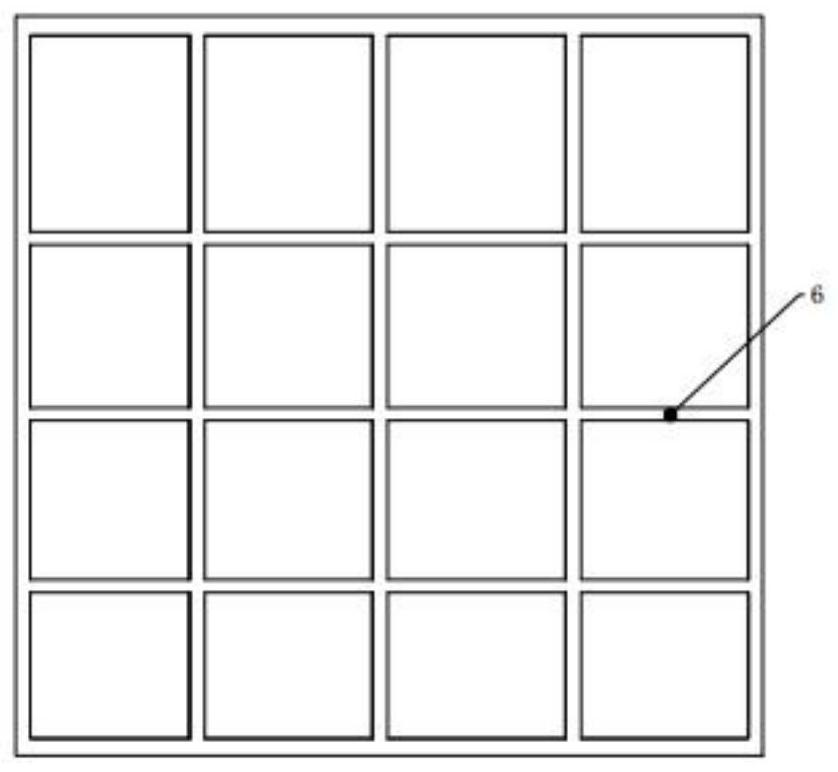
[0065] In step (3), using a double-sided positioning photolithography process, a chip dicing line corresponding to the P side is made on the N side, and the ohmic contact metal film layer 3 on the N side is corroded by an corrosive solution to form a dicing line 6, and the dicing line 6 The width is 30 μm.

[0066] In step (5), the etching conditions are as follows: feed the etching gas as Cl 2 and Ar, where Cl 2 The gas flow rate of Ar is 100 sccm, the gas flow rate...


PUM

PropertyMeasurementUnit
thicknessaaaaaaaaaa
thicknessaaaaaaaaaa
widthaaaaaaaaaa

Abstract

The invention relates to a cutting method of a GaAs-based LED chip. The cutting method comprises the following specific steps: (1) grinding a front-end semi-finished product COW of the GaAs-based LEDchip; (2) evaporating an ohmic contact metal film layer on the N surface of the COW; (3) corroding the ohmic contact metal film layer on the N surface of the COW to form a cutting channel; (4) coatingthe P surface of the COW with a curing adhesive; (5) transferring the COW to ICP etching equipment, and carrying out ICP dry etching; (6) covering the N surface of the COW with a blue film; and (7) removing the curing adhesive on the P surface of the COW to obtain the independent chip. According to the method, the ICP etching technology is adopted to cut the N surface of the front process semi-finished product COW of the GaAs-based LED chip, the ohmic contact metal film layer is adopted as a mask to perform ICP dry etching, the cutting efficiency is high, the phenomena of P collapse and N collapse do not occur, and the appearance yield is 10-20% higher than that obtained through mechanical cutting.

Description

technical field [0001] The invention relates to a method for cutting GaAs-based LED chips, belonging to the technical field of semiconductor chip cutting. Background technique [0002] With the rapid development of social economy, energy issues have gradually become a global issue; LED chips have the characteristics of high brightness, rich colors, low power consumption, and long life. LEDs are widely used in lighting, display, backlight and other fields. With the improvement of technology, the photoelectric conversion efficiency has been significantly improved. Compared with 3 years ago, the existing technology can produce the same brightness on 50% of the chip area, so the chip area is gradually reduced, that is, a smaller area can obtain the same brightness. Brightness, the chip is getting smaller and smaller. [0003] The cutting process in the preparation process of gallium arsenide-based LED chips is to divide the whole chip into a single chip. At present, GaAs-based ...

Claims


Application Information

Patent Timeline
Patent Type & Authority Applications(China)
IPC IPC(8): H01L33/00
CPCH01L33/0062
Inventor 彭璐张兆梅林伟王成新
Owner SHANDONG INSPUR HUAGUANG OPTOELECTRONICS
Why Eureka
Try Eureka